EN
 EN
 DA
 NL
 FI
 FR
 DE
 IT
 JA
 KO
 NO
 PL
 PT
 RO
 RU
 ES
 SV
 TL
 ID
 SK
 UK
 VI
 TH
 TR
 FA
 BE
 LA
 UZ

CVD Coating
CVD Coating Solutions – High-Purity SiC, TaC & PYC Coatings for Semiconductor Thermal Fields
Core Introduction
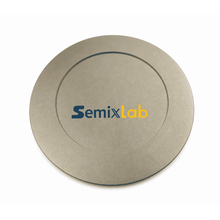
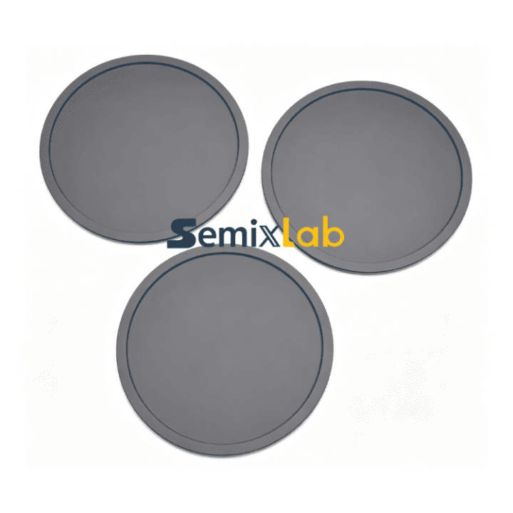
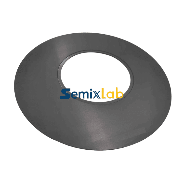
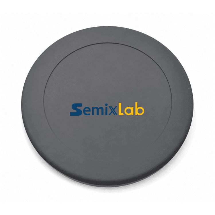
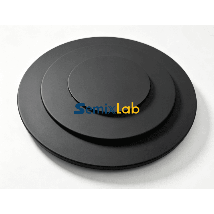
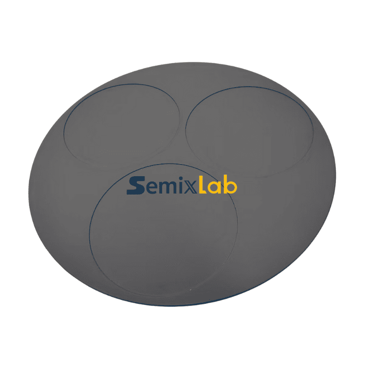
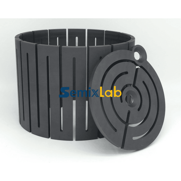
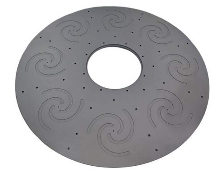
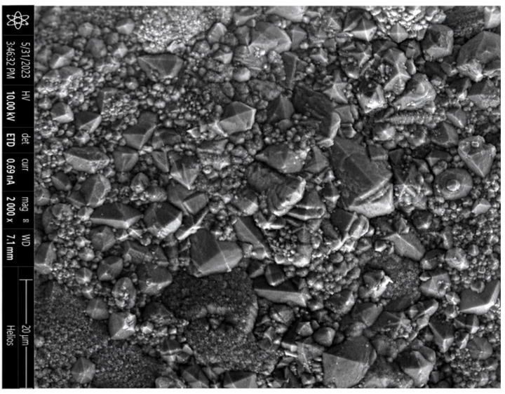
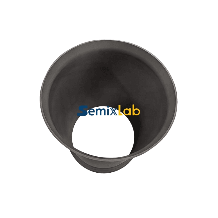
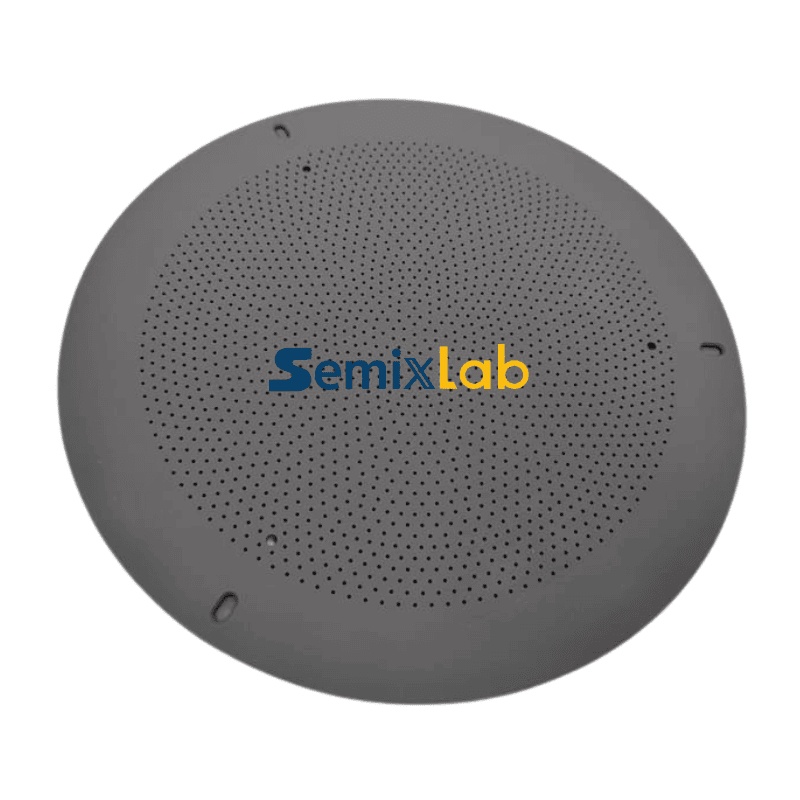
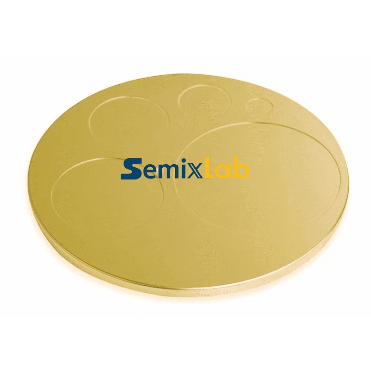
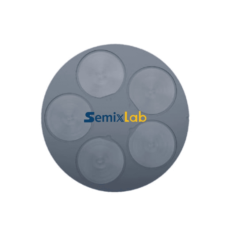
SemiXLab specializes in advanced chemical vapor deposition (CVD) coatings engineered for the most demanding semiconductor processes. Our CVD-SiC (silicon carbide), CVD-TaC (tantalum carbide), and PYC / PG (pyrolytic carbon / pyrolytic graphite) coatings deliver excellent film uniformity, interfacial adhesion strength, and ultra-high-purity dense structures.
These coatings protect graphite substrates used in wafer epitaxy and high-temperature corrosive environments, significantly extending component life while minimizing particle generation. Through proprietary process control and independent CVD equipment development, we achieve stable coating thickness, excellent crystal orientation uniformity, and outstanding resistance to hydrogen, ammonia, and halogen process gases.
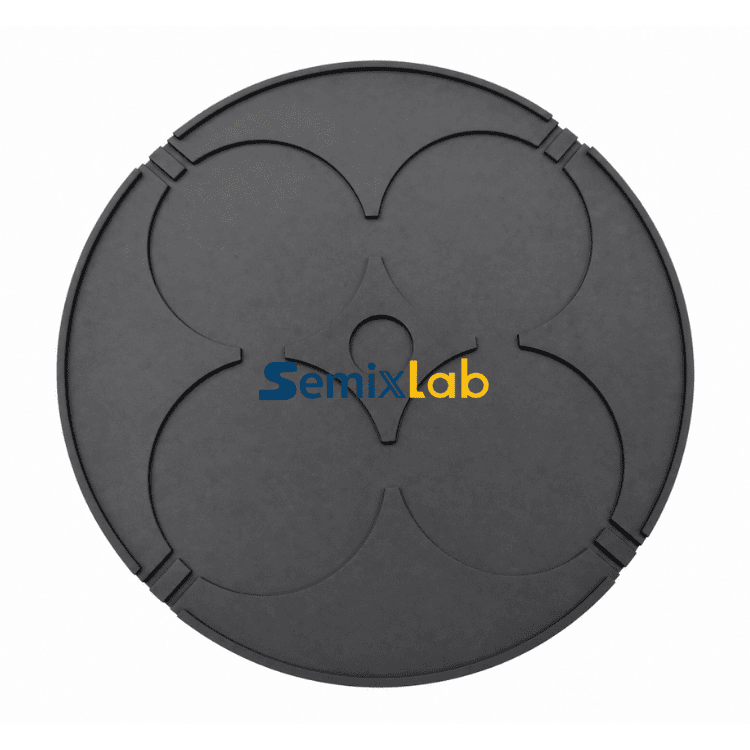
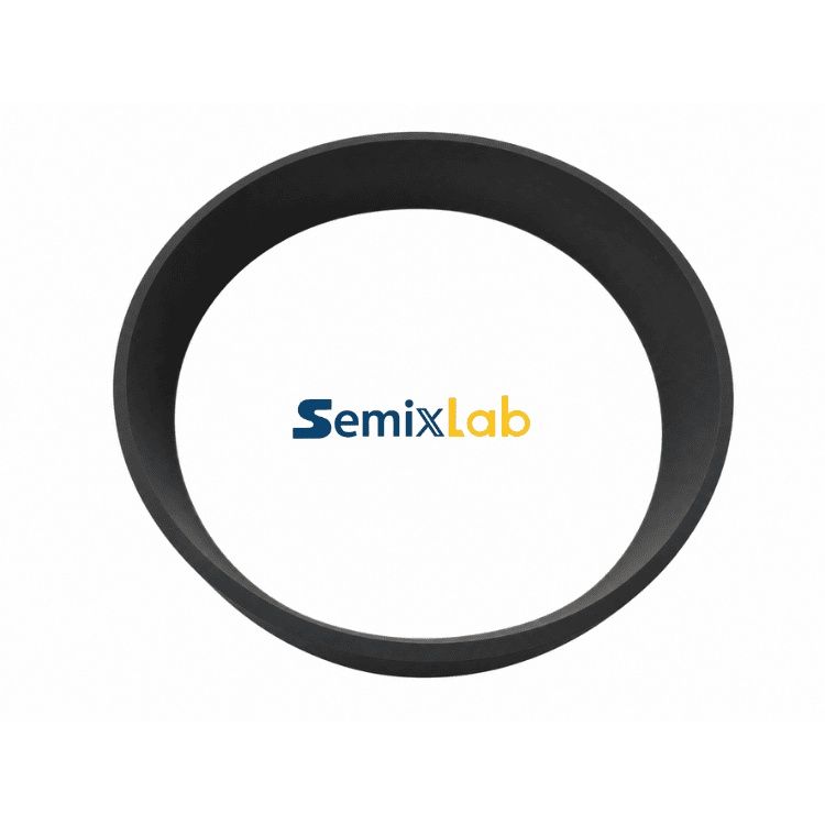
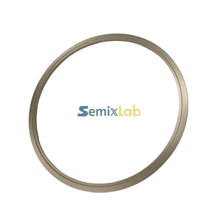
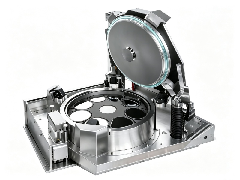
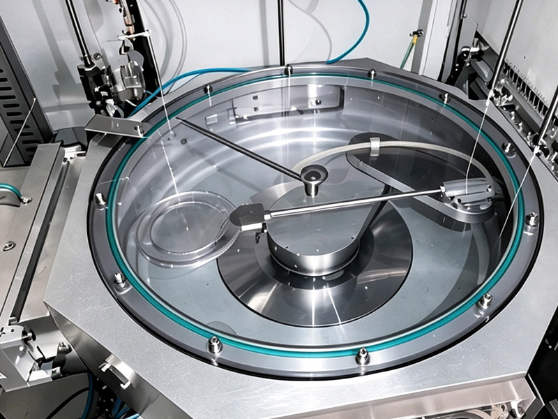
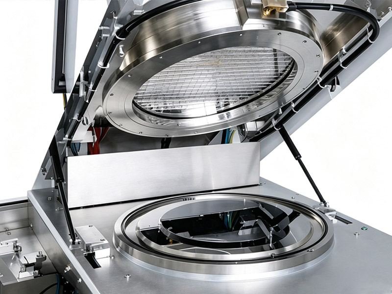
Key advantages include high-temperature corrosion resistance, particle-free surfaces (reducing wafer contamination risk), and CTE-matched design with the substrate to ensure dimensional stability during thermal cycling. Our coatings are widely applied to MOCVD susceptors, epitaxial wafer carriers, LED / SiC / GaN film deposition platforms, and other critical thermal-field components.
Key Specifications
| Parameter | CVD SiC | CVD TaC | PG / PyC | Glass Carbon |
|---|---|---|---|---|
| Density | 3.21 g/cm³ | 14.3 g/cm³ | ~2.25 g/cm³ | 1.42–1.54 g/cm³ |
| Hardness | 2500 HV | 2000 HK | 1.2 GPa | 230–340 HV |
| Purity | 99.99995% | High purity | ≤5 ppm | High purity (low ash) |
| Thermal Cond. | 300 W·m⁻¹·K⁻¹ | 9–22 W/(m·K) | — | 4.6–6.3 W/(m·K) |
| CTE | 4.5×10⁻⁶ /K | 6.3×10⁻⁶ /K | — | 2.6–3.5×10⁻⁶ /K |
| Max Temp. | ~2100°C (subl. 2700°C) | <2500°C | High | Inert 2800–3000°C; air ~600°C |
| Typical Thickness | Customizable | 35±10 μm (≥20 μm) | 30–100 μm | 50–100 μm |
| Key Advantages | High thermal conductivity, mature process, cost-effective | Ultra-high density, extreme temp, chemical stability | High purity, orientable, low hardness | Gas-tight, strong corrosion resistance, low particles |
| Applications | SiC/GaN epi, MOCVD, RTP, diffusion, high-temp heaters | SiC PVT crystal growth, ultra-high-temp epi rings, thermal fields | Thermal-field assist, insulation, high-purity surfaces | Etch/plasma, strong corrosion, ultra-high-purity carriers |
Application Scenarios
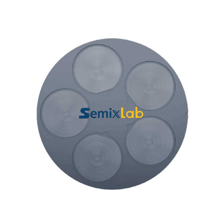
- MOCVD epitaxial susceptors (GaN, GaAs, SiC, LED)
- Epitaxial wafer carriers and rotating susceptors
- LED / SiC / GaN film deposition components
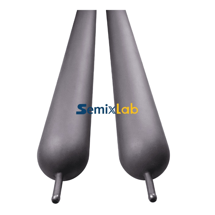
- High-temperature furnace parts, heaters, showerheads, RTP trays
Application Schematic
CVD Coating