EN
 EN
 DA
 NL
 FI
 FR
 DE
 IT
 JA
 KO
 NO
 PL
 PT
 RO
 RU
 ES
 SV
 TL
 ID
 SK
 UK
 VI
 TH
 TR
 FA
 BE
 LA
 UZ

Emerging Technologies – Advanced Materials R&D for Next‑Generation Semiconductor & MEMS Applications
Core Introduction
The “Emerging Technologies” section showcases SemiXLab’s R&D capabilities for technology‑driven customers seeking customized breakthroughs. We focus on materials innovations that address emerging process challenges in third‑/fourth‑generation semiconductors, MEMS sensors, and ultra‑high‑temperature extreme environments.
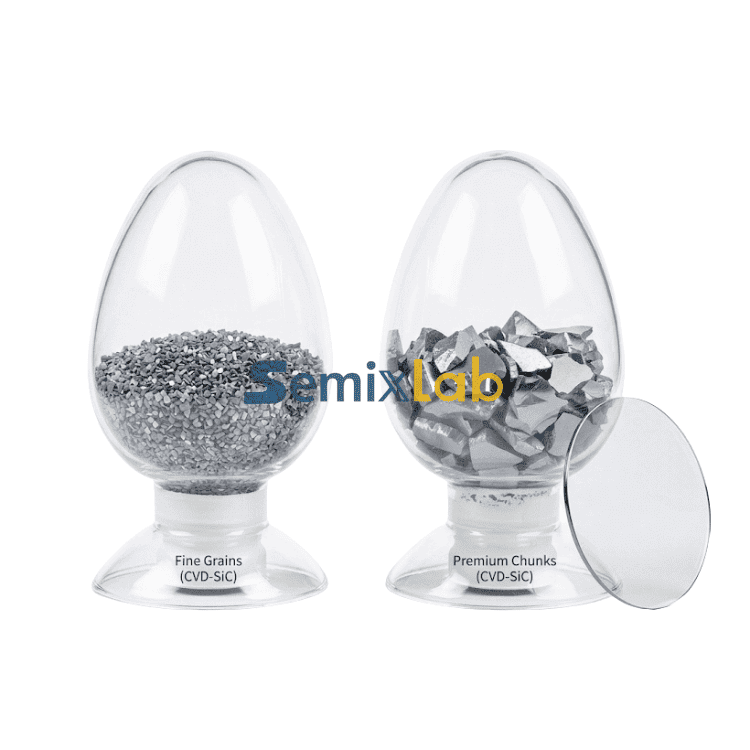
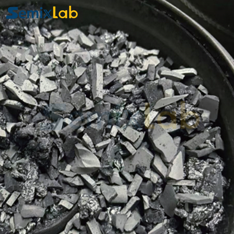
- High‑purity CVD‑SiC feedstock (SiC Crystal Growth Raw Material): 7N‑grade chunks/blocks optimized for SiC PVT crystal growth.
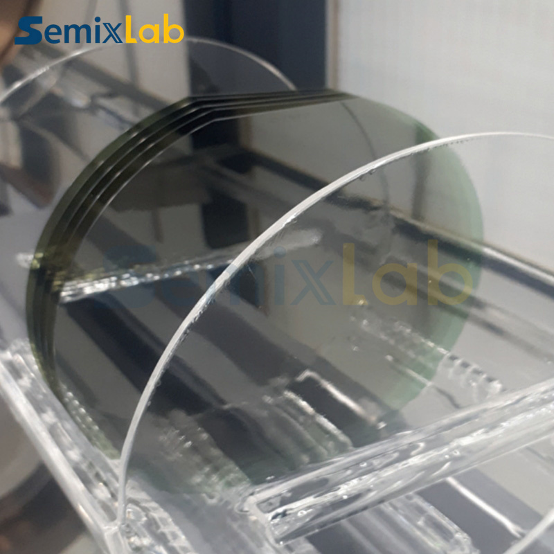
- 3C‑SiC Wafer: cubic‑phase silicon carbide wafers for power and high‑frequency devices.
- Piezoelectric MEMS structural components (PZT‑on‑Si / SOI), gradient coating technology, and next‑generation carbon‑based nano TIMs.
All innovations are supported by patent portfolios, rigorous laboratory validation (GDMS / SIMS / CMM), and flexible joint‑development (JDEV) collaboration models. Customers can partner from concept and pilot stages through to scaled production.
Spotlight: High‑Purity CVD‑SiC Feedstock (SiC Crystal Growth Raw Material)
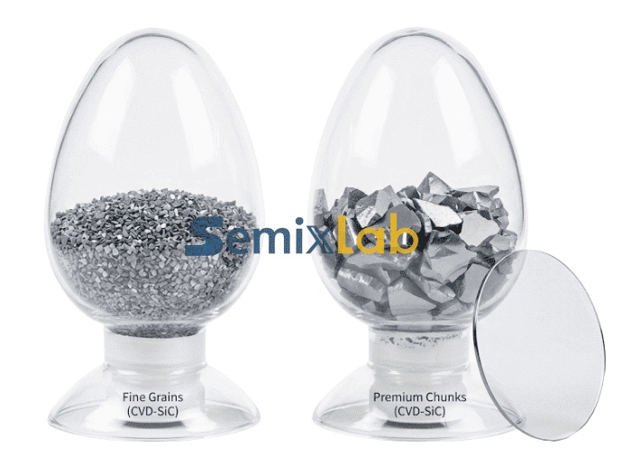
Produced via fluidized‑bed CVD process (methyltrichlorosilane precursor), this ultra‑high‑purity β‑SiC feedstock is specifically designed for PVT SiC single‑crystal growth. Compared with conventional Acheson‑process feedstock, it offers significant advantages:
| Key Parameter | Typical Value / Notes |
|---|---|
| Purity | 99.9999950% (7N+ grade, based on GDMS detection limits) |
| Nitrogen Content (N) | 4.98 × 10¹⁵ Atom/cm³ ≈ 0.05 ppm (SIMS measured, no extra purification required) |
| Particle Size | Average 4–10 mm (significantly larger than domestic Acheson feedstock <2.5 mm) |
| Si/C Molar Ratio | Closer to 1:1, reducing Si‑vapor‑pressure‑induced defects |
| Utilization Rate | >50% (4.5 kg feedstock yields ~3.5 kg crystal ingot) |
| Main Advantages | Large high‑density particles → higher charge per crucible volume; ultra‑low N → suitable for semi‑insulating; uniform evaporation → better process control; higher yield & lower defects |
This feedstock effectively addresses the shortcomings of conventional Acheson material (insufficient purity, overly fine particles, Si/C deviation) and is an ideal source material for high‑performance SiC single‑crystal growth. See the secondary page SiC Crystal Growth Raw Material for details.
Other Technology Highlights
| Technology Area | Description |
|---|---|
| High‑Purity CVD‑SiC Feedstock | 7N‑grade chunks/blocks, N ≈0.05 ppm, optimized for SiC PVT |
| 3C‑SiC Wafer | Cubic‑phase silicon carbide wafers for advanced power & high‑frequency devices |
| Piezoelectric MEMS Structures | PZT‑on‑Si / SOI components for advanced sensors and actuators |
| Gradient Coating Technology | Functionally graded coatings improving adhesion and high‑temperature performance |
| Carbon‑Based Nano TIM | Next‑generation thermal interface materials for high‑power packaging |