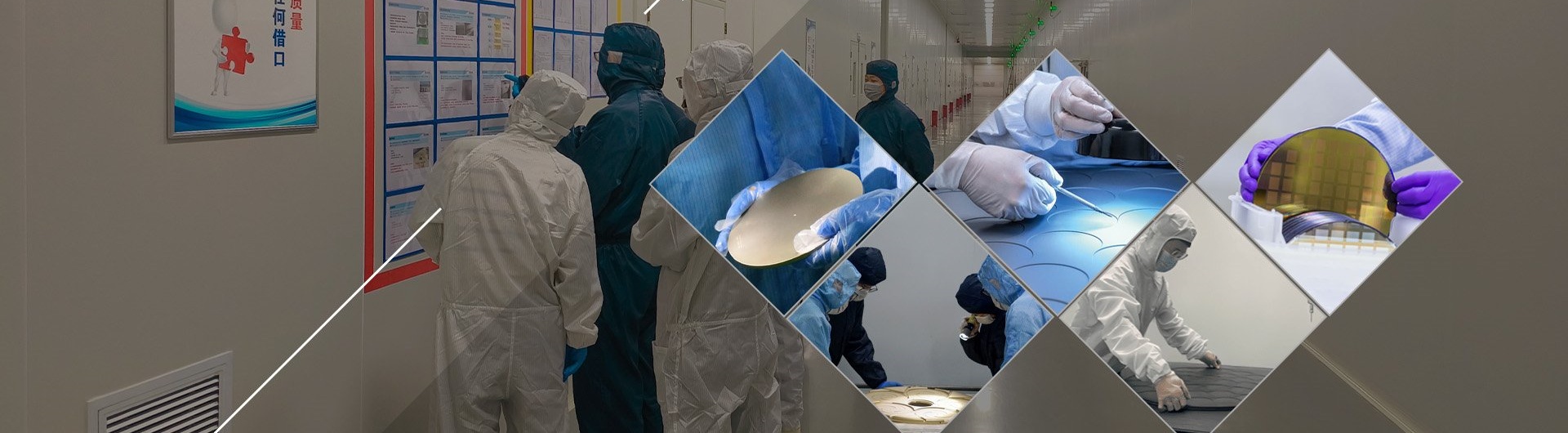
Based on customer physical samples, SemiXLab performs end‑to‑end mapping at its Zhuji production base—from geometric reverse engineering to material‑level analysis. The goal is clear: enable Form‑Fit‑Function substitution so that remanufactured parts truly match in installation dimensions, process compatibility, and chamber lifetime. For SiC source materials used in PVT, the focus is on purity, morphology, and sublimation‑related properties to ensure reproducible crystal‑growth performance.
Submit Sample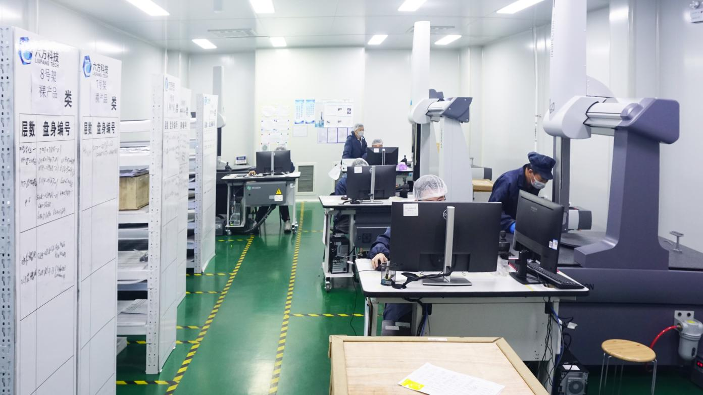
Dimensions, coating cross‑sections, substrate CTE, and purity data are all captured in one go and feed directly into subsequent material selection and mass‑production process packages.
| Mapping Dimension | Method / Equipment | Customer Value |
|---|---|---|
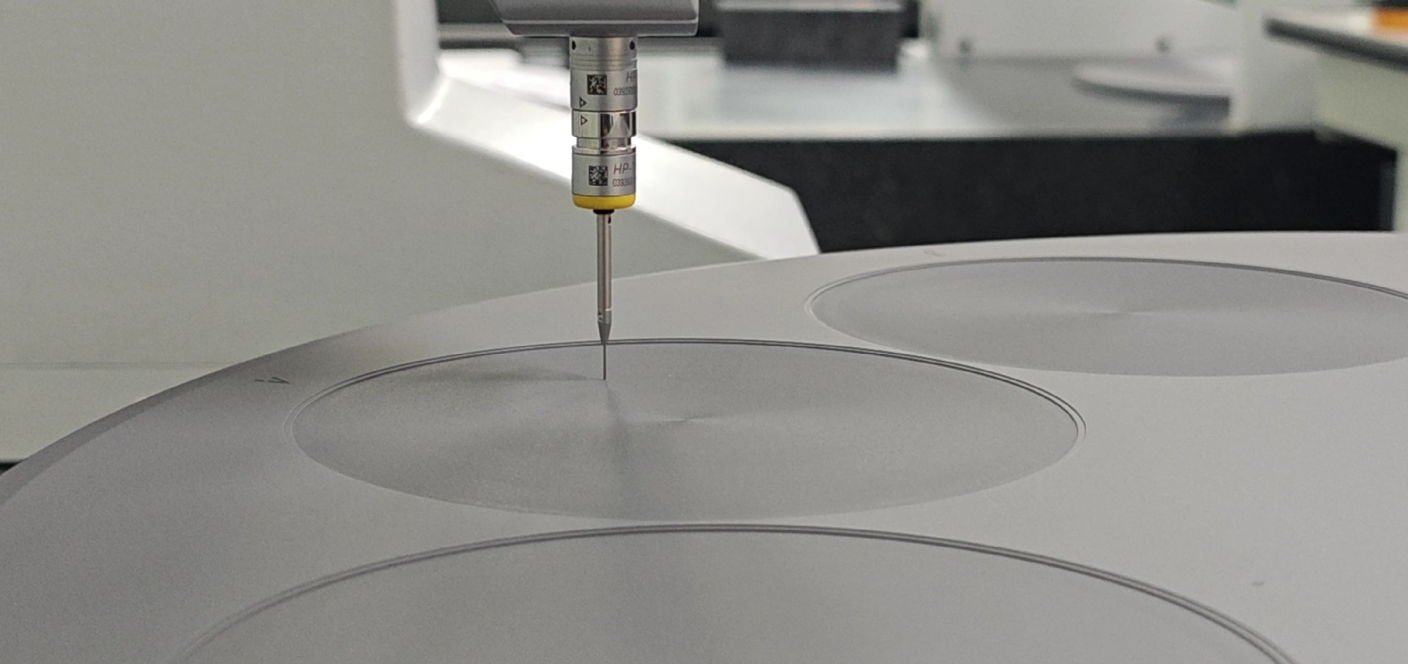
| Dimensions & Geometric Tolerances | CMM + optical 3D scanning | Full‑dimension point‑cloud reconstruction; installation with zero deviation; CNC precision down to 3 μm |
| Surface & Flatness | White‑light interferometry / optical profilometry | Meets wafer‑carrying and sealing requirements |
| Edge R / Chamfer | High‑magnification profile mapping | Optimizes coating coverage; reduces high‑temperature delamination |
| Substrate & CTE Matching | Density / grain size / CTE evaluation | Coating remains crack‑ and peel‑free under thermal cycling |
| Coating Cross‑Section & Interface | XRF + SEM cross‑section | Quantified film‑thickness uniformity and adhesion strength |
| Phase Structure / Crystallinity | XRD (β‑SiC / TaC stoichiometry) | Evidence‑based corrosion resistance and high‑temperature phase stability |
| Purity & Trace Elements | GDMS / SIMS | Metallic impurities<5 ppm; Source feedstock can be verified at 7N‑level purity |
| Source Morphology & Particle Size | SEM / particle‑size analysis / bulk density | CVD SiC Source block size and morphology controllable; favors stable PVT sublimation |

 EN
 EN
 DA
 NL
 FI
 FR
 DE
 IT
 JA
 KO
 NO
 PL
 PT
 RO
 RU
 ES
 SV
 TL
 ID
 SK
 UK
 VI
 TH
 TR
 FA
 BE
 LA
 UZ