EN
 EN
 DA
 NL
 FI
 FR
 DE
 IT
 JA
 KO
 NO
 PL
 PT
 RO
 RU
 ES
 SV
 TL
 ID
 SK
 UK
 VI
 TH
 TR
 FA
 BE
 LA
 UZ

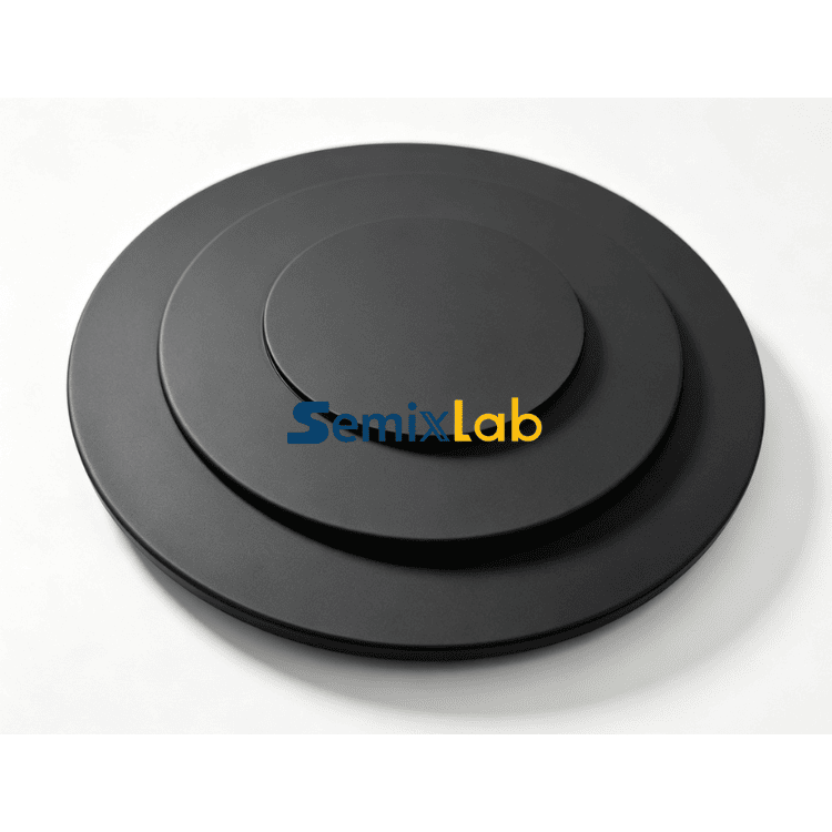
CVD SiC Coated Graphite Susceptor for Epitaxy
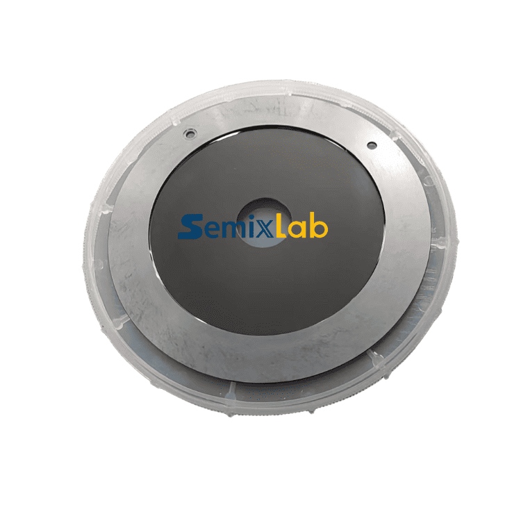
Semixlab CVD SiC Coated Graphite Susceptor for Epitaxy is made from high-purity graphite with a CVD SiC surface. The circular, stepped design provides a defined position for the wafer during MOCVD growth. It is commonly used for GaN and GaAs epitaxy, where surface cleanliness and consistent thermal conditions are important.
Description
Product Advantages & Features
● SiC-coated working surface
The CVD SiC layer forms the process-facing surface of the susceptor and helps protect the graphite from the surrounding process environment.
● High-purity graphite body
The graphite substrate provides the thermal response required for high-temperature epitaxy and can be machined to match different equipment designs.
● Recessed wafer position
The stepped structure gives the wafer a fixed seating area, helping maintain its position during processing.
● Made for epitaxy equipment
The susceptor can be manufactured for different wafer diameters, pocket dimensions and equipment configurations used in GaN and GaAs production.
Customization, Quality Assurance & Support
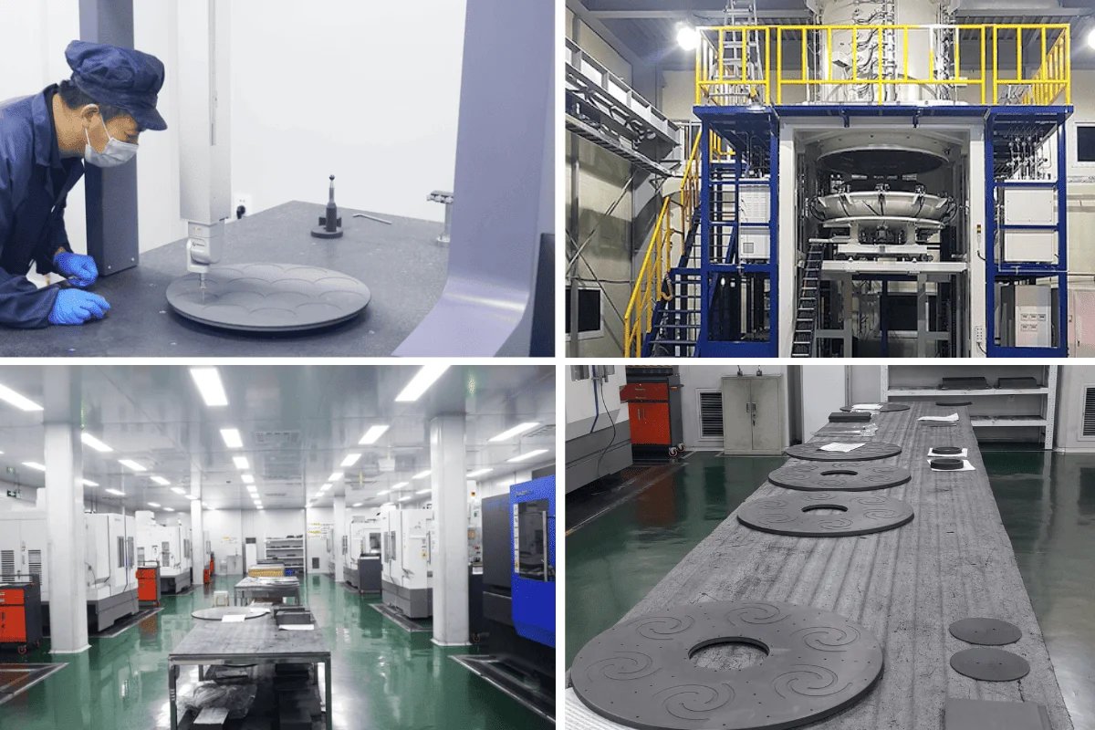
We can manufacture the graphite body, wafer pocket and CVD SiC coating according to your drawing, wafer size or equipment requirements, with inspection carried out before shipment; send us your drawing or application details for a quotation.
Specifications
Specifications & Product Categories
| Item | Specification |
| Product | CVD SiC Coated Graphite Epitaxy Susceptor |
| Graphite Grade | High-Purity Isostatic Graphite |
| Surface Coating | CVD SiC |
| Typical Coating Thickness | 100 ± 20 μm |
| SiC Purity | Up to 99.99995% |
| Structure | Stepped / Recessed |
| Typical Processes | GaN and GaAs Epitaxy, MOCVD |
| Wafer Size | Available according to requirement |
| Dimensions | Customizable |
Applications
The susceptor is used in MOCVD systems for GaN and GaAs epitaxial growth, where the wafer needs stable support throughout the deposition process.
Typical applications include compound semiconductor epitaxy, LED wafer growth and GaN-based device development.
Different pocket sizes and surface configurations can be supplied for specific wafer sizes and reactor designs.
Our Services

Semixlab Product Shop