EN
 EN
 DA
 NL
 FI
 FR
 DE
 IT
 JA
 KO
 NO
 PL
 PT
 RO
 RU
 ES
 SV
 TL
 ID
 SK
 UK
 VI
 TH
 TR
 FA
 BE
 LA
 UZ

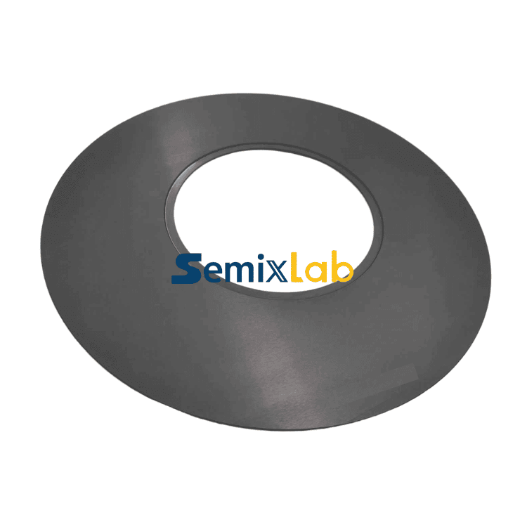
MOCVD Wafer Carrier
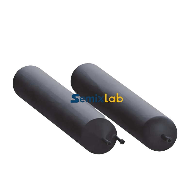
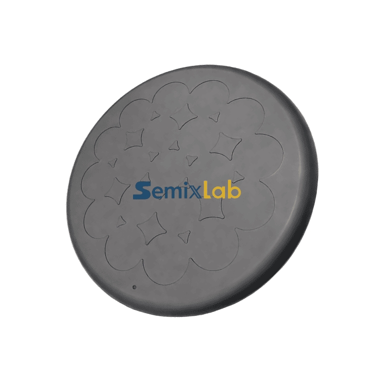
Semixlab MOCVD wafer carriers (also known as susceptors or wafer trays) are critical consumable components inside Metal-Organic Chemical Vapor Deposition reactors. They provide stable mechanical support, uniform heat transfer, and chemical isolation for wafers during high-temperature epitaxial growth of GaN, AlN, AlGaN, SiC, GaAs and related compound semiconductor layers.
Description
Product Overview
Semixlab offers two complementary material platforms:
• Solid SiC Carriers: Fully dense, high-purity silicon carbide produced by advanced CVD or sintering routes. Ideal for the most demanding high-temperature and high-purity processes where zero graphite outgassing is required.
• CVD SiC Coated Graphite Susceptors: High-density isostatic graphite substrate protected by a dense, uniform CVD silicon carbide coating (typically 50–150 µm). Combines excellent thermal conductivity of graphite with superior corrosion and particle resistance of SiC.
Both platforms are manufactured under strict clean-room and purity control, with CNC precision machining down to ±3 µm tolerance, supporting mainstream MOCVD platforms, and custom planetary or single-wafer reactors.
Key Features & Technical Advantages
• Exceptional Temperature Uniformity: Thermal conductivity up to 300 W·m⁻¹·K⁻¹ (CVD SiC) and optimized emissivity ensure wafer surface temperature variation typically < ±1 °C, critical for thickness and composition control.
• Ultra-High Purity & Low Particle Generation: Metal impurities controlled to < 1 ppm (ICP-MS); ash content ≤ 5 ppm. Dense SiC surface minimizes particle adhesion and gas-phase contamination that cause memory effects or yield loss.
• Superior Chemical & Thermal Stability: Resistant to H₂, NH₃, HCl, Cl₂ and high-temperature process gases. Operating temperature capability up to 1600–1800 °C depending on configuration.
• Precision Geometry & Surface Finish: Five-axis CNC machining achieves flatness, concentricity and pocket depth control essential for multi-wafer planetary systems. Optional polished surface Ra ≤ 0.2–0.5 µm.
• Long Service Life & Recoating Support: Dense coating integrity and low residual stress extend usable cycles. Semixlab also provides professional cleaning and recoating services to maximize total cost of ownership.
• Full Customization: Pocket layouts, satellite/planet designs, single-wafer or multi-wafer formats (2"–12"), edge rings, and thermal-field matching available on request.
Typical Material Properties
| Property | CVD SiC Coating | Solid SiC |
| Crystal Structure | β-SiC (FCC), mainly (111) | β / α-SiC dense polycrystal |
| Density | ≈ 3.21 g/cm³ | ≥ 3.15 g/cm³ |
| Purity | ≥ 99.99995 % | ≥ 99.999 % typical |
| Thermal Conductivity | ≈ 300 W·m⁻¹·K⁻¹ | 120–200+ W·m⁻¹·K⁻¹ |
| CTE (RT–1000 °C) | ≈ 4.5 × 10⁻⁶ K⁻¹ | ≈ 4.0–4.5 × 10⁻⁶ K⁻¹ |
| Max. Service Temp. | ≤ 1600–1800 °C (inert) | ≤ 1600–2000 °C (inert) |
| Hardness | ~2500 HV | High (SiC typical) |
Note: Exact values depend on grade, coating thickness and process route. Custom datasheets available upon request.
Why Semixlab – Manufacturing + Trading Integration
Semixlab is a vertically integrated supplier of advanced thermal-field materials and coatings for compound semiconductors. Unlike pure traders or pure factories, we control both process development and production capacity:
• In-house CVD equipment & process know-how: Proprietary vertical CVD reactors and coating recipes deliver dense, low-stress SiC layers with excellent uniformity and adhesion.
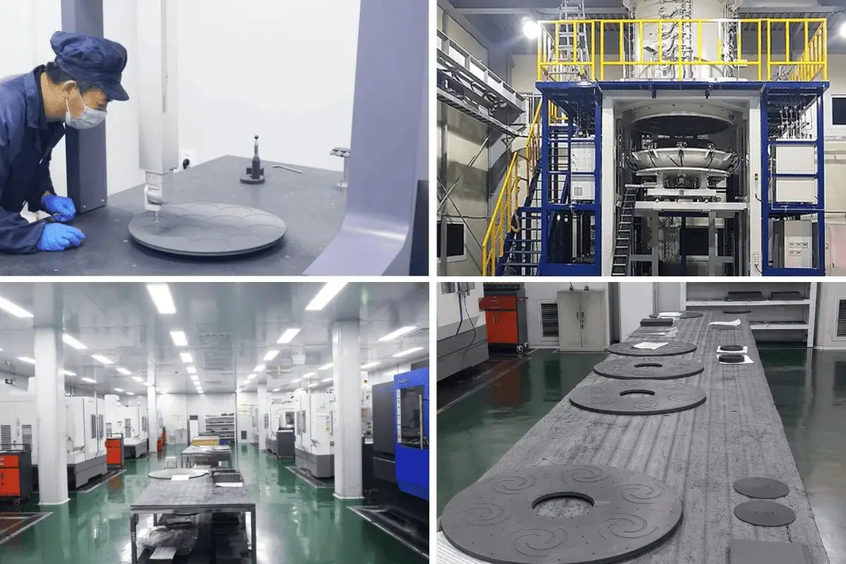
• Precision machining capability: Dedicated diamond tooling and five-axis CNC for Solid SiC and coated graphite, achieving tight geometric tolerances and low residual stress.
• Closed-loop quality control: Incoming material purity, coating thickness mapping, residual stress, particle and metallic impurity inspection, plus full traceability.
• Application engineering support: We match carrier design to your reactor thermal profile, gas-flow pattern and process chemistry — not just supply a standard part.
• Complementary services: Professional cleaning (AlN residue removal & memory-effect control), recoating, and lifetime extension programs reduce your total cost of ownership.
Manufacturing Excellence – Stress Control & Yield
For Solid SiC annular and disk carriers, residual thermal stress has historically caused cracking during diamond grinding (open-roughing yield often < 20 %). Semixlab solved this by:
1. Switching from conventional horizontal CVD furnaces to high-symmetry vertical CVD reactors optimized by CAE thermal/flow simulation.
2. Implementing staged high-temperature annealing to relieve residual stress (> 70 % reduction).
3. Result: open-roughing yield improved from < 20 % to > 95 %, enabling stable volume supply of crack-free Solid SiC carriers for 12-inch and advanced nodes.
This vertical-furnace + stress-management capability is a core differentiator for customers who require reliable Solid SiC wafer carriers and focus rings.
Get Started
Need high-performance MOCVD wafer carriers with proven temperature uniformity, low particle generation and stable supply? Contact Semixlab today for samples, technical datasheets or a customized quotation.
Website: https://www.semixlab.com
Email / Technical inquiry: Available via website contact form or sales team
Related services: CVD SiC Coated Graphite Parts Professional Cleaning (AlN residue removal & memory-effect control) | Solid SiC Focus Rings & Edge Rings for Dry Etch
Applications
Applications & Use Cases
• GaN / AlGaN / AlN MOCVD epitaxy for power devices, RF, and UV-LED
• SiC and silicon epitaxy processes
• LED (blue, green, UV, deep-UV) epitaxial growth
• Planetary, vertical, and single-wafer MOCVD reactors (Aixtron, Veeco, LPE, Nuflare, ASM, TEL compatible designs)
• High-temperature diffusion, oxidation and annealing carriers where chemical inertness is required
Our Services

Semixlab Product Shop