EN
 EN
 DA
 NL
 FI
 FR
 DE
 IT
 JA
 KO
 NO
 PL
 PT
 RO
 RU
 ES
 SV
 TL
 ID
 SK
 UK
 VI
 TH
 TR
 FA
 BE
 LA
 UZ

Silicon Parts
Product Overview
Semixlab supplies precision silicon components for plasma etching, deposition, thermal processing and wafer‑handling equipment. Silicon provides process compatibility with silicon wafer manufacturing while offering controllable electrical properties, thermal performance and purity for chamber‑facing consumables.
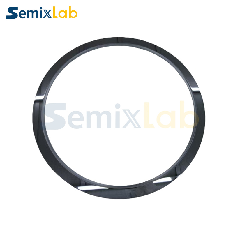
Available products include silicon focus rings, edge rings, electrodes, plates, gas‑distribution components and custom replacement parts.
Key Features & Advantages
- Semiconductor‑Grade Material: Controlled material purity helps reduce unwanted metallic contamination near the wafer.
- Tailored Electrical Properties: Conductivity type, resistivity and crystal orientation can be selected for the process requirement.
- Precision Geometry: Tight control of thickness, flatness, concentricity, hole patterns and edge profiles supports stable chamber performance.
- Controlled Surface Finish: Grinding, lapping, etching and polishing options are available for process‑facing surfaces.
Technical Specifications
| Parameter | Standard / Typical Value |
|---|---|
| Material | Monocrystalline / Polycrystalline Silicon |
| Conductivity Type | Intrinsic / P‑Type / N‑Type |
| Crystal Orientation | <100> / <111> |
| Resistivity | Drawing or process specified |
| Density | Approx. 2.33 g/cm³ |
| Thermal Conductivity | 130‑150 W/(m·K) |
| Surface Finish | Ground / Lapped / Etched / Polished |
Final electrical and dimensional specifications are confirmed according to the approved drawing and material grade.
Typical Applications
- · Focus rings, edge rings and electrodes for plasma etch chambers
- · Silicon plates and gas‑distribution parts for deposition equipment
- · Chamber consumables for wafer fabrication systems
- · Custom parts for semiconductor equipment maintenance and process R&D
Customization Capabilities
Semixlab supports customized silicon type, conductivity, resistivity, orientation, diameter, thickness, hole pattern, groove profile, edge shape and surface roughness. Production can begin from an approved CAD drawing or authorized sample mapping.
Quality Assurance & Expertise
- · Raw‑material documentation and traceability
- · Resistivity, orientation and dimensional verification as specified
- · Surface‑roughness and visual‑defect inspection
- · Controlled cleaning, packaging and qualification‑sample support
Resources & Call to Action
- Engineering Consultation: Provide the tool model, process gas, plasma conditions and current component failure mode.
- Request a Quote: Send your approved drawing, material requirements and quantity for review.
- Product Resources: View Semixlab product information and semiconductor material solutions.
Silicon Parts
Silicon parts are mainly used because they match the wafer material. That alone makes them useful, since it reduces the chance of introducing unwanted differences into the process. They are common in etching and deposition environments. Performance is generally stable, although lifetime can vary quite a bit depending on how harsh the process is.
With better machining and surface treatment, these parts have improved over time. Even so, they’re not always chosen for durability, but more for compatibility and process consistency.