EN
 EN
 DA
 NL
 FI
 FR
 DE
 IT
 JA
 KO
 NO
 PL
 PT
 RO
 RU
 ES
 SV
 TL
 ID
 SK
 UK
 VI
 TH
 TR
 FA
 BE
 LA
 UZ

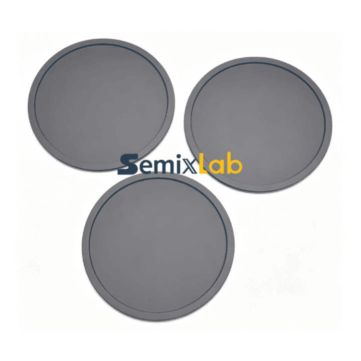
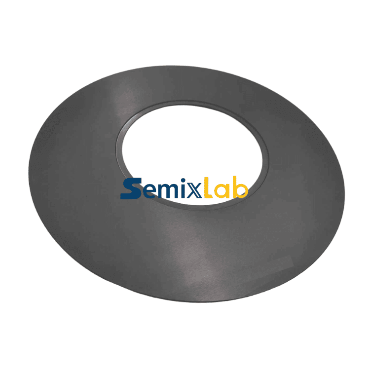
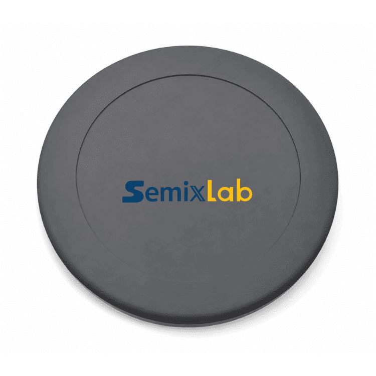
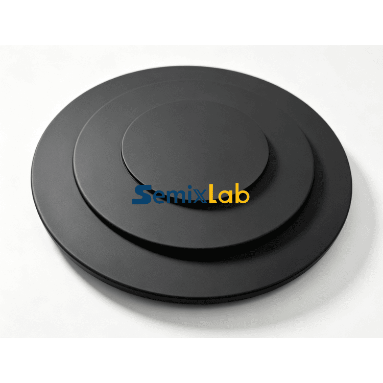
CVD Silicon Carbide (SiC) Coating
Product Overview
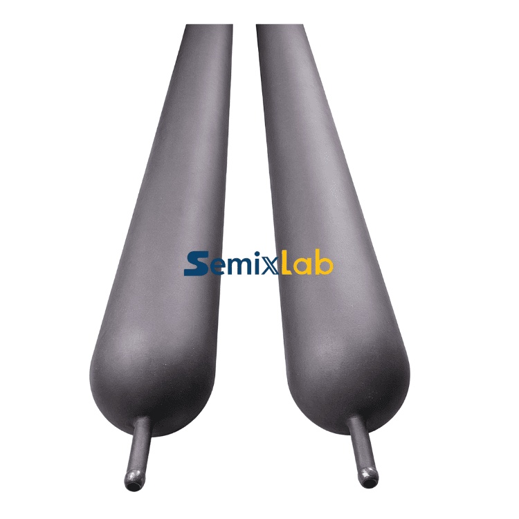
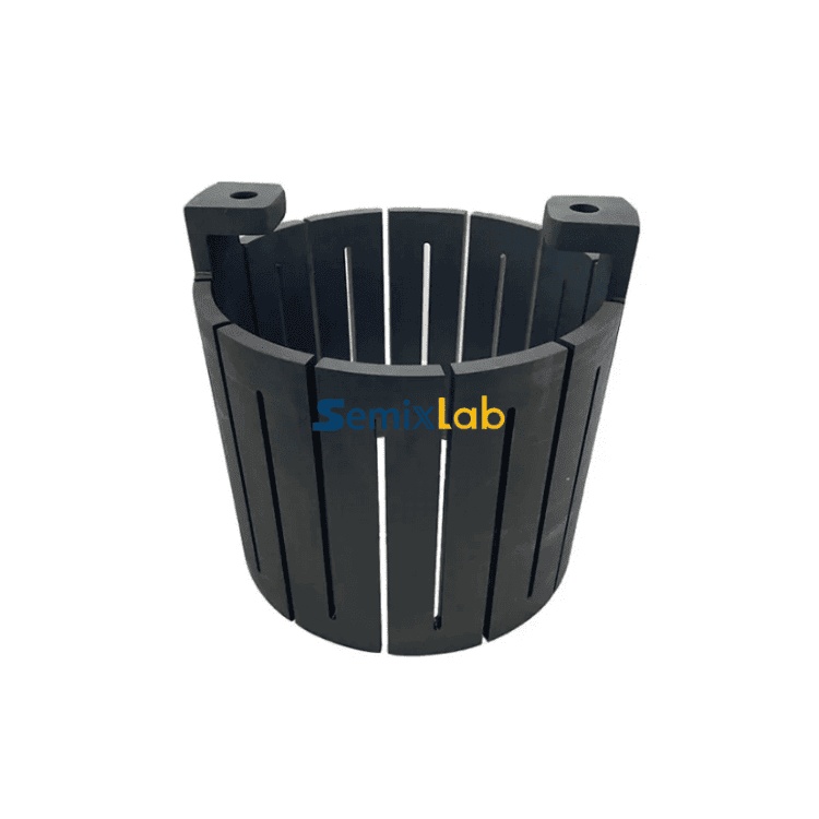
Semixlab’s Chemical Vapor Deposition Silicon Carbide (CVD SiC) coating is engineered specifically for the most demanding semiconductor front‑end processes. Utilizing ultra‑pure vapor‑phase reactants, we deposit a highly dense, polished‑grade β‑phase (β‑SiC) face‑centered cubic crystal structure onto isotropic high‑purity graphite substrates.
With a purity level reaching 99.999% (5N) and total metallic impurities under 1 ppm, this coating delivers exceptional oxidation resistance, chemical inertness, and thermal uniformity at temperatures up to 1600°C. It prevents particle shedding and outgassing from graphite substrates, significantly boosting wafer epitaxy (Epi) yields.
Key Features & Advantages
- Ultra‑High Purity & Low Outgassing: Achieves 99.999% purity with total impurities < 1 ppm as verified by SIMS, eliminating heavy metal cross‑contamination on Si/SiC epitaxial layers at elevated temperatures.
- Isotropic Dense Structure: Features a relative density > 99.8% with zero micropores or cracks, forming a gas‑tight barrier against aggressive gases like HCl, NH₃, and H₂.
- Perfect CTE Matching: Tailored deposition process aligns the Coefficient of Thermal Expansion (CTE: 4.5–4.8 × 10⁻⁶/K) with isostatic graphite, ensuring zero delamination or cracking through 500+ rapid thermal cycles (RTC).
- Superior Plasma Etch Resistance: Maintains an extremely low erosion rate (< 0.02 µm/min) under aggressive fluorine‑based (CF₄/NF₃) and chlorine‑based plasma cleaning environments.
Technical Specifications
| Parameter | Standard / Value | Test Method / Condition |
|---|---|---|
| Crystal Structure | Face‑Centered Cubic β‑SiC | XRD Analysis |
| Purity | ≥ 99.999% (5N) | GDMS / SIMS Depth Profiling |
| Density | ≥ 3.20 g/cm³ | Archimedes Principle |
| Coating Thickness | 80 µm – 120 µm (Customizable) | Eddy Current / Metallographic Section |
| Thermal Conductivity | ≥ 200 W/(m·K) | Flash Method (25°C) |
| Adhesion Strength | ≥ 150 MPa | Scratch Adhesion Test |
| Surface Roughness | Ra ≤ 0.8 µm (Polished Ra ≤ 0.1 µm) | Profilometer |
Typical Applications
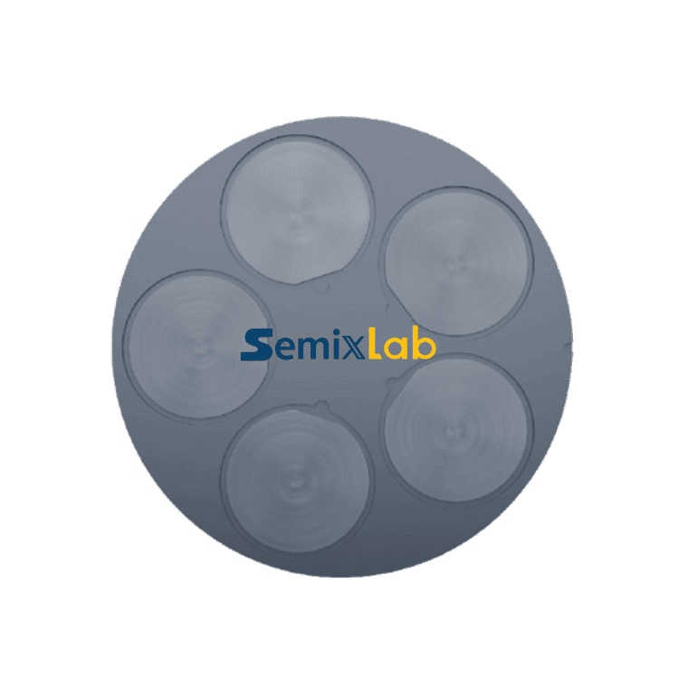
- Silicon Epitaxy (Si‑Epi): Susceptors, satellite rings, and guide plates used in single‑crystal silicon epitaxy growth.
- Wide‑Bandgap Semiconductors (SiC / GaN Epi): Susceptors and baseplates for high‑temperature SiC epitaxial growth reactors (e.g., LPE, Aixtron, Nuflare).
- MOCVD LED & Power Devices: Wafer carriers and platters for GaN‑on‑Si and GaN‑on‑Sapphire manufacturing.
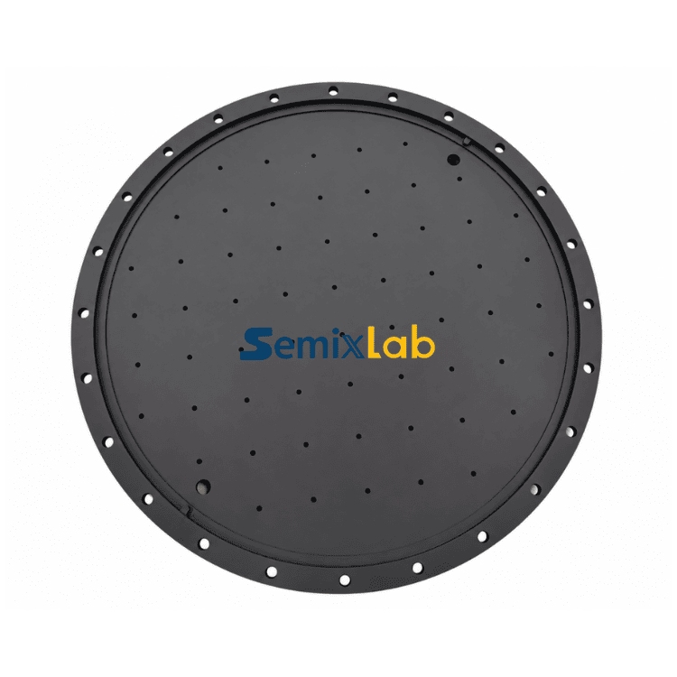
- Dry Etching Equipment: Etch chamber components, gas distribution plates (showerheads), and protective shrouds.
Customization Capabilities
Semixlab operates proprietary CVD reactors integrated with computational fluid dynamics (CFD/FEA) for thermal and gas flow optimization.
- Complex Geometries: Achieves 100% uniform thickness deposition across micro‑holes (aspect ratios up to 1:5), blind holes, deep grooves, and large disks up to 800 mm in diameter.
- Tailored Thickness: Coating thickness can be tailored from 30 µm to 300 µm to meet specific operational lifespan requirements.
- Precision Post‑Processing: Precision mirror polishing, edge chamfering, and full CMM dimensional inspection services are available.
Quality Assurance & Expertise
- ISO Certified & Semiconductor‑Grade Control: Certified under ISO 9001:2015 and ISO 14001:2015, operating dedicated Class 100 (ISO 5) cleanroom facilities for cleaning and packaging.
- Comprehensive In‑House Testing: Every batch includes full analytical reports for GDMS impurities, XRD phase purity, and thickness uniformity.
- Decades of exquisite craftsmanship experience: Led by senior semiconductor materials experts, our products are qualified in leading global Foundries and IDM supply chains.
Technical Resources & Next Steps
- Engineering Consultation: Looking to optimize coating performance for specific toolsets (AMAT, ASM, Lam Research, etc.)?
- Request a Quote: Submit your CAD drawings and process specifications for an engineering evaluation within 24 hours.
- Download Resource: Download the CVD SiC Coating Product Datasheet (PDF)
CVD Silicon Carbide (SiC) Coating
CVD SiC coating is basically a silicon carbide layer deposited on graphite, and it’s widely used in epitaxy tools where both temperature and cleanliness matter. In real production lines, you’ll often see it in systems from AIXTRON, ASM/LPE, Veeco, as well as some AMAT-related platforms. What makes it useful is not just the temperature resistance, but the overall stability during long runs. Under typical epitaxy conditions — hydrogen, ammonia, or even chlorinated gases — the coating stays relatively stable and protects the graphite underneath. That helps keep the thermal field more consistent and reduces the chance of particles showing up during growth.
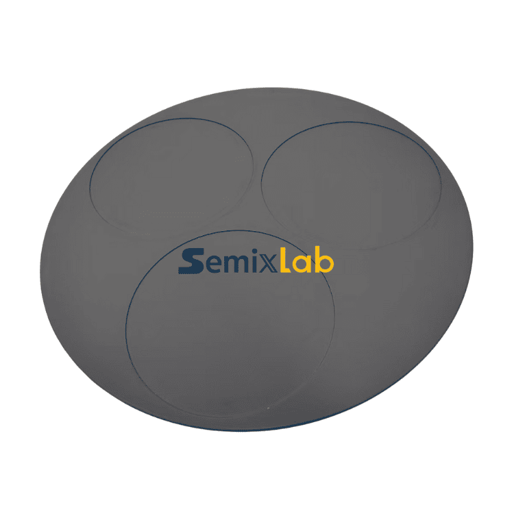
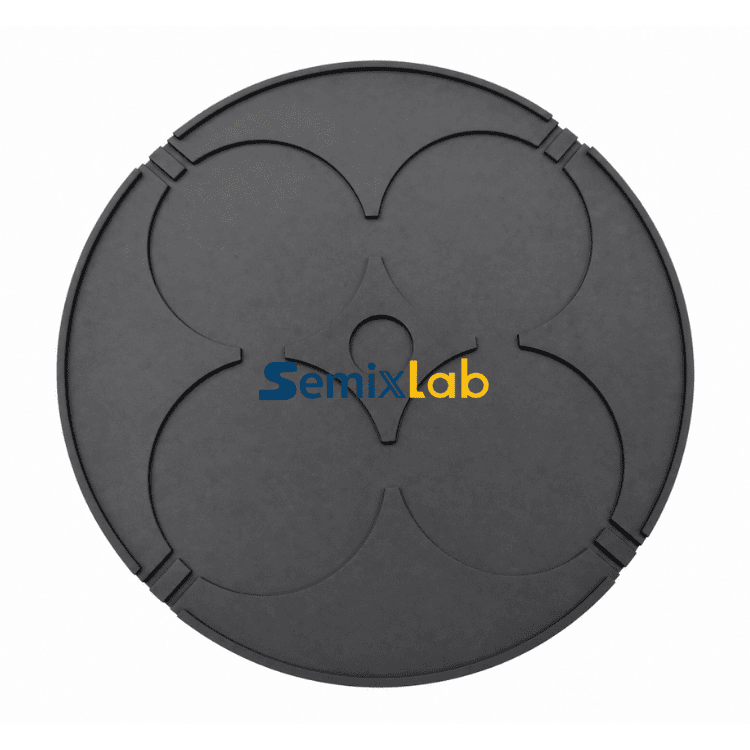
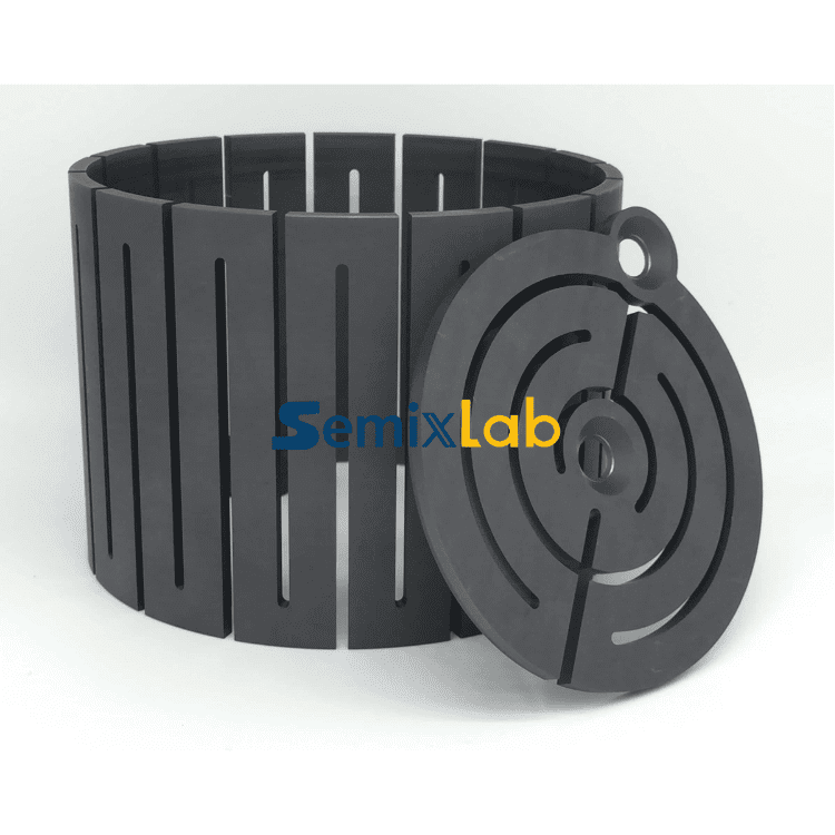
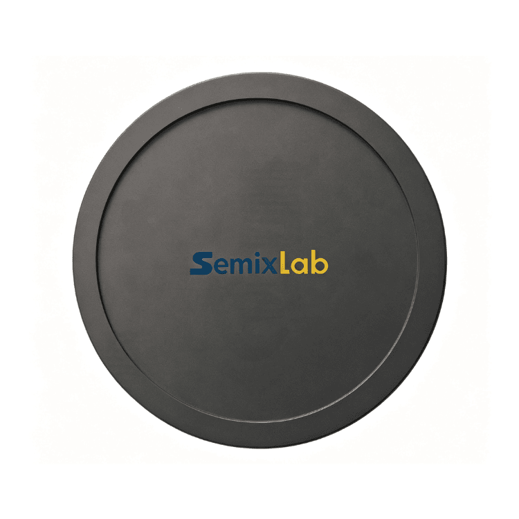
Most of the time, the coating is applied to parts like susceptors, wafer carriers, graphite rings, or half-moon components. These are all directly involved in wafer heating or positioning, so any small instability can affect yield. For that reason, coated parts are often treated as consumables that still need to be reliable over multiple cycles, especially in 4 to 12 inch production.