EN
 EN
 DA
 NL
 FI
 FR
 DE
 IT
 JA
 KO
 NO
 PL
 PT
 RO
 RU
 ES
 SV
 TL
 ID
 SK
 UK
 VI
 TH
 TR
 FA
 BE
 LA
 UZ
Abstract
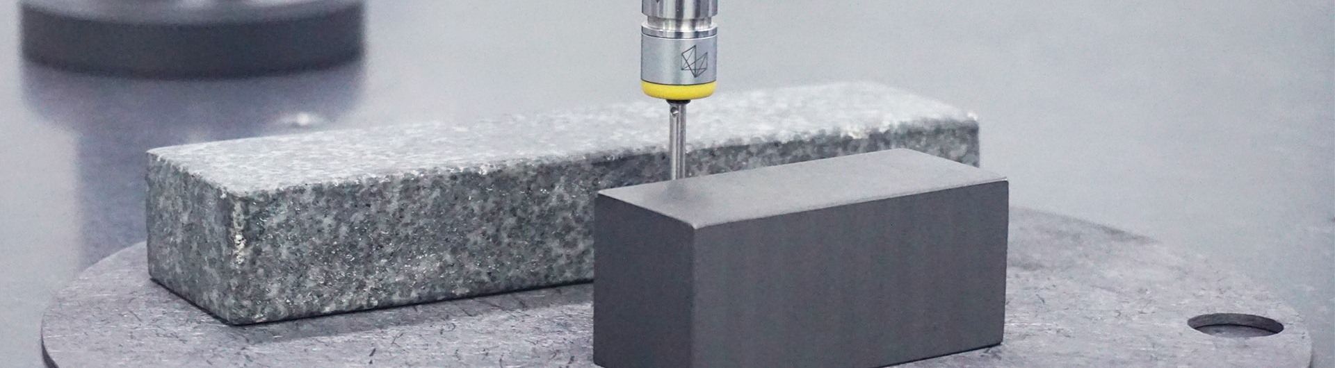
This technical white paper explains why 5N, 6N, and 7N purity grades alone are insufficient for qualifying SiC source material for PVT crystal growth. It examines element-specific impurities including N, B, Al, Fe, Ti, and V, explains the complementary roles of GDMS and SIMS, discusses semi-insulating compensation mechanisms, and provides a practical COA and multi-run supplier qualification framework.
For SiC single-crystal growth by physical vapor transport (PVT), the purity of the source material cannot be defined by 5N, 6N, or 7N alone.
These grades indicate the approximate total impurity ceiling:
· 5N: 99.999% purity, ~10 ppm total impurities
· 6N: 99.9999% purity, ~1 ppm
· 7N: 99.99999% purity, ~0.1 ppm
But PVT crystal performance depends on which impurities remain, not only how many total impurities are present.
The technically relevant specification is therefore:
Total Purity + Element-Specific Impurity Budget + Analytical Method + Lot Consistency + PVT Qualification
For power-device substrates, conductive 4H-SiC, high-resistivity material, and semi-insulating SiC, the acceptable impurity window can be very different.
The most critical source-related elements typically include:
N, B, Al, Fe, Ti, and V.
The main engineering conclusion of this white paper is:
A purity grade defines the impurity ceiling; an impurity budget defines whether the source is suitable for PVT crystal growth.
1. Why 5N, 6N, and 7N Are Only the Starting Point
The N-grade system is useful because it provides a simple first comparison between high-purity materials.
| Purity Grade | Nominal Purity | Approx. Impurity Ceiling |
| 5N | 99.999% | 10 ppm |
| 6N | 99.9999% | 1 ppm |
| 7N | 99.99999% | 0.1 ppm |
For procurement, this is convenient.
For crystal-growth engineering, it is incomplete.
Two source materials can both be specified as 6N while containing very different impurity populations.
For example:
Source A
· N relatively high
· B very low
· Al very low
Source B
· N very low
· B and Al relatively higher
Their nominal total purity may be similar, but their behavior in PVT growth may not be equivalent because nitrogen is a donor while boron and aluminum act as acceptors.
The same problem becomes more important when comparing 6N and 7N materials.
A 7N claim without:
· analytical scope;
· detection limits;
· element-specific results;
· nitrogen data;
· lot-to-lot statistics
is much less useful than a well-characterized 6N material.
This is particularly relevant because published PVT studies show that elemental impurities do not behave identically during vapor transport. Al, B, Fe, and Ti have been detected in both source powders and grown wafers, while their relative concentrations changed differently during growth.
Therefore, source qualification should begin with:
How many impurities remain?
but immediately continue with:
Which impurities remain?
2. From Total Purity to an Element-Specific Impurity Budget
PVT growth is a high-temperature transport process.
The source material does not simply transfer its original chemical composition directly into the crystal.
Instead:
→ Source Material
→ Sublimation
→ Gas-Phase Transport
→ Interaction with Graphite Hot Zone
→ Impurity Segregation / Incorporation
→ Growing Crystal
This means the final impurity content of the boule is determined by several coupled mechanisms.
A practical impurity model is:
Source Impurity + Hot-Zone Contamination × Transport Efficiency × Incorporation Behavior = Crystal Impurity
Published experiments show that impurities such as Al, B, Fe, and Ti can originate from the source, while graphite crucibles and insulation materials may also contribute contamination.
For this reason, high-purity SiC source material should be specified using an impurity budget.
| Element | PVT Relevance |
| N | Shallow donor; often dominant residual donor |
| B | Acceptor; compensation-sensitive |
| Al | Acceptor; affects conductivity balance |
| Fe | Transition-metal / deep-level contamination |
| Ti | Deep-level impurity |
| V | Deep-level dopant used in some SI-SiC routes |
The engineering value of a high-purity source therefore depends not only on reducing the total impurity level, but on reducing the electrically relevant impurity population.
This is why an advanced PVT specification should be written as:
Total Purity Requirement plus Maximum N / B / Al / Fe / Ti / V Levels rather than using a single purity number.
3. Nitrogen, Boron, Aluminum, Fe, Ti, and V: Why Their Roles Are Different
1. Nitrogen
Nitrogen deserves separate treatment because it is one of the most important residual donors in SiC.
In nominally undoped PVT growth, classic work found nitrogen to remain the dominant residual impurity, while Al, B, V, and Ti were present at much lower levels.
For n-type substrates, nitrogen may be intentionally introduced.
For semi-insulating SiC, however, nitrogen becomes a major constraint because every residual donor must eventually be compensated.
Therefore:
Low total impurity does not automatically mean low donor concentration.
A material can look “high purity” chemically while still carrying too much nitrogen for a narrow semi-insulating process window.
2. Boron and Aluminum
Boron and aluminum act as acceptors.
Their importance lies in compensation balance.
A PVT boule is not chemically static during growth. Published work on B- and V-doped PVT growth showed that nitrogen concentration decreased along the growth direction, while boron-related electrical behavior changed with growth time.
This means that incoming source chemistry influences not only the starting condition, but also the axial electrical uniformity of the final boule.
3. Fe and Ti
Fe and Ti are transition-metal impurities and may introduce electrically active deep levels.
Even at trace concentrations, they may matter for high-resistivity or lifetime-sensitive material.
For engineering qualification, their value should therefore be linked to:
· carrier concentration;
· resistivity;
· compensation strategy;
· deep-level behavior;
· wafer uniformity.
4. Vanadium
Vanadium requires a different interpretation.
It is not simply an undesirable contaminant.
In some semi-insulating SiC processes, V is intentionally used as a deep-level compensating dopant.
However, vanadium has a finite solubility range. Excess V may cause precipitation and nonuniformity, while insufficient V may fail to compensate residual donors.
Therefore:
The target is not “minimum V.” The target is controlled V relative to the donor–acceptor background.
4. GDMS and SIMS: Why Analytical Method Is Part of the Specification
A purity claim is only as useful as the analytical method behind it.
For semiconductor-grade PVT source material, a COA should clearly state:
· test method;
· sample location;
· detection limit;
· reporting limit;
· whether values are measured or calculated.
1. GDMS
Glow Discharge Mass Spectrometry is highly useful for broad elemental screening of high-purity solids.
Its main value is the ability to build a wide impurity profile covering many metallic and semi-metallic contaminants.
For SiC source qualification, GDMS is suitable for monitoring elements such as:
B, Al, Fe, Ti, V, Cr, Ni, Cu, Ca, Na
and related trace contaminants.
2. SIMS
Secondary Ion Mass Spectrometry is especially valuable when ultra-low-level dopants or light elements must be measured.
For SiC, this is particularly important for nitrogen.
In advanced high-purity material, nitrogen can become difficult to quantify because analytical background approaches the sample signal.
SIMS is therefore often used for:
· low-level nitrogen;
· dopant concentration;
· depth profiling;
· axial or radial concentration studies.
The practical qualification model is:
GDMS = Broad Impurity Budget
SIMS = Low-Level N / Dopant Verification
For technical procurement, the following question is critical:
Was nitrogen actually measured, or was it implicitly included in the advertised total purity?
This distinction becomes extremely important at 6N and especially 7N.
5. Why Higher Purity Does Not Automatically Produce Better Crystal Quality
It is tempting to assume:
5N → 6N → 7N → continuously better crystal but PVT growth is not that simple.
Published work comparing different SiC source purities found that impurity content influenced micropipes and dislocation populations. One study reported that the effect on micropipe density became much smaller below about the 1 ppm impurity level, while dislocations continued to decrease as source purity improved further.
This is important because it shows two things.
First:
Higher purity can improve crystal quality.
Second:
Different defect populations do not respond identically to purity.
Crystal quality is also governed by:
· seed quality;
· thermal gradient;
· supersaturation;
· growth rate;
· interface shape;
· graphite purity;
· gas atmosphere;
· crucible design;
· thermal stress.
Therefore, high-purity source material should be viewed as a process-control variable, not a standalone guarantee of low defects.
This leads to a more useful engineering statement:
Purity reduces one part of the defect-generation risk, but does not replace thermal-field and growth-interface control.
For this reason, a 7N source should not automatically be selected over a 6N source unless its improvement is measurable in the target PVT system.
6. Semi-Insulating SiC: The Strongest Case for Element-Level Control
Semi-insulating SiC is where the weakness of a simple N-grade becomes most obvious.
The electrical state of SI-SiC depends on compensation among:
Residual Donors
↔
Acceptors
↔
Deep Levels
In classical vanadium-compensated material, V can act as a deep compensating center.
But if residual nitrogen is too high, the amount of vanadium required to compensate it may approach practical limits.
Published PVT work showed that nitrogen was the dominant residual impurity and that dopant homogeneity was essential for achieving stable semi-insulating behavior.
Work on B and V incorporation further showed that dopant concentration changes along the boule, meaning that semi-insulating growth is inherently a dynamic compensation problem, not a static chemistry problem.
A more realistic SI-SiC material strategy is therefore:
→ Low N Background
→ Controlled B / Al
→ Controlled V or Intrinsic Compensation
→ High-Purity Graphite Hot Zone
→ Stable Axial Incorporation
This explains why the correct engineering question is not:
“Is 7N required?”
but:
“Is the donor–acceptor–deep-level balance sufficiently controlled across the full boule?”
That question is far more meaningful than the number of “9s.”
7. COA Qualification: What Should a Semiconductor-Grade SiC Source Supplier Provide?
A production-grade COA should convert “high purity” into measurable acceptance criteria.
A recommended minimum structure is:
| COA Item | Recommended Requirement |
| Total purity | Guaranteed minimum |
| Nitrogen | Separate result + method |
| B / Al | Lot-specific value or maximum |
| Fe / Ti / V | Lot-specific value or maximum |
| Other metals | Broad elemental scan |
| Free Si / Free C | Where process-relevant |
| GDMS / SIMS method | Explicitly stated |
| Detection limits | Reported for critical elements |
| Lot number | Full traceability |
| Historical consistency | Multi-lot data |
For technical buyers, the most important distinction is:
Typical versus Guaranteed
A “typical 7N” result does not mean every production lot is guaranteed to meet 7N.
Likewise: Below Detection Limit
does not mean: Zero.
The detection limit itself must therefore become part of supplier qualification.
For CVD-derived SiC feedstock, one further issue should be controlled:
The final crushed and cleaned feedstock—not only the as-deposited CVD material—should be analyzed.
Crushing, sizing, cleaning, handling, and packaging can all introduce contamination.
Engineering Decision Guide
For practical material selection:
5N can be suitable for:
· exploratory R&D
· less purity-sensitive development;
· non-critical crystal-growth trials.
It should not automatically be assumed suitable for advanced high-resistivity or SI-SiC growth.
6N represents a strong semiconductor-grade baseline for many PVT programs.
It becomes technically meaningful when accompanied by:
· N data;
· B/Al limits;
· transition-metal limits;
· stable multi-lot COA results.
7N provides a much lower theoretical impurity ceiling.
Its greatest value appears in:
· ultra-high-purity research;
· semi-insulating development;
· processes where source contamination is already a dominant limitation.
But 7N is only useful if:
the measurement capability is good enough to prove it.
Technical FAQ
1. What purity SiC source material is required for PVT crystal growth?
There is no universal minimum. 6N+ is a useful benchmark for advanced semiconductor-grade source materials, but the final specification should be based on element-specific impurity limits and the crystal's electrical target.
2. Is 7N always better than 6N?
No. A 7N material without reliable N/B/Al/Fe/Ti/V data may be less controllable than a well-characterized 6N source.
3. Which impurity matters most?
There is no single universal answer, but nitrogen is especially important because it is a common residual donor. B, Al, Fe, Ti, and V should also be controlled according to the target material.
4. Why are GDMS and SIMS both needed?
GDMS is useful for broad trace-element analysis, while SIMS is especially valuable for low-level nitrogen and dopant measurement.
5. What matters most for semi-insulating SiC?
The key factor is the donor–acceptor–deep-level balance, not simply total purity.
6. What should a buyer request from a supplier?
A complete COA, guaranteed impurity limits, analytical methods, detection limits, multi-lot consistency data, and sufficient material for multi-run qualification.
Conclusion
For PVT SiC crystal growth, purity should not be reduced to a contest between 5N, 6N, and 7N.
The correct engineering model is:
→ Purity Grade
→ Impurity Ceiling
→ Element-Specific Impurity Budget
→ GDMS / SIMS Verification
→ PVT Transport and Incorporation
→ Electrical / Defect Response
→ COA Qualification
→ Multi-Run Crystal Validation
A 7N label can be useful.
A controlled impurity budget is more useful.
A repeatable impurity budget that produces stable crystal performance is what ultimately matters.
References
1. Shin, D. G. et al., “Impurity Behavior of High Purity SiC Powder during SiC Crystal Growth,”
2. Bickermann, M. et al., “On the Preparation of Semi-Insulating SiC Bulk Crystals by the PVT Technique,”
3. Bickermann, M. et al., “Incorporation of Boron and Vanadium during PVT Growth of 6H-SiC Crystals,”
4. Heo, S. et al., “Influence of Impurities in SiC Powder on High Quality SiC Crystal Growth.”
Table of Contents
- Why 5N, 6N, and 7N Are Only the Starting Point
- From Total Purity to an Element-Specific Impurity Budget
- Nitrogen, Boron, Aluminum, Fe, Ti, and V: Why Their Roles Are Different
- GDMS and SIMS: Why Analytical Method Is Part of the Specification
- Why Higher Purity Does Not Automatically Produce Better Crystal Quality
- Semi-Insulating SiC: The Strongest Case for Element-Level Control
- COA Qualification: What Should a Semiconductor-Grade SiC Source Supplier Provide?
- Engineering Decision Guide
- Technical FAQ
- Conclusion
Founded in 2018, Semixlab Technology Co.,Ltd is a technology-based enterprise focusing on the research and development, production and sales of advanced materials. It is a world-leading semiconductor material manufacturer.