EN
 EN
 DA
 NL
 FI
 FR
 DE
 IT
 JA
 KO
 NO
 PL
 PT
 RO
 RU
 ES
 SV
 TL
 ID
 SK
 UK
 VI
 TH
 TR
 FA
 BE
 LA
 UZ
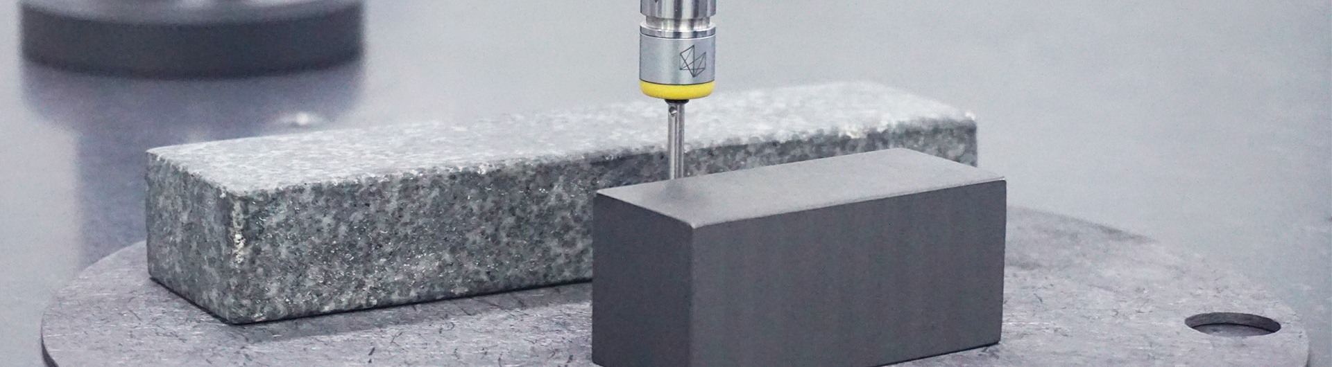
In brief: Silicon carbide rode the EV wave. GaN is capturing RF and fast chargers. Now aluminum nitride (AlN) — with a 6.2 eV bandgap and theoretical breakdown field of ~15.4 MV/cm — is emerging as the true fourth-generation ultra-wide-bandgap platform for ultra-high-voltage power, extreme RF, and deep-ultraviolet optoelectronics. Chinese producers have already achieved stable 2-inch AlN single-crystal mass production. The same high-temperature materials challenges that defined SiC (high-purity powder, long-life crucibles, precise thermal gradients) now define AlN. For materials suppliers, this is the next demand curve.
1. Why Aluminum Nitride Is the Fourth-Generation Semiconductor
AlN is a wurtzite ultra-wide-bandgap semiconductor whose fundamental material metrics sit well above both SiC and GaN:
| Material Property | SiC (4H) | GaN | AlN | Advantage |
| Bandgap (eV) | 3.26 | 3.4 | 6.2 | Highest |
| Breakdown field (MV/cm) | ~2.5–3 | ~3.3 | 12–15.4 | ~5× higher |
| Thermal conductivity (W/m·K) | ~370–490 | ~200–230 | ~320–340 | Excellent |
| Dielectric constant | ~9.7 | ~9.5 | ~8.5–8.7 | Lower |
| Saturation velocity (10⁷ cm/s) | ~2 | ~2.5 | ~2 | Comparable |
These properties translate directly into device-level advantages: higher voltage ratings with thinner drift layers, superior thermal management under extreme power density, and the ability to emit and detect deep-ultraviolet light (UVC < 280 nm). Target applications include:
• Ultra-high-voltage power electronics (grid, data-center solid-state transformers, traction beyond 3.3 kV)
• Extreme RF & radar (military, 6G base stations, aerospace)
• Deep-UV optoelectronics (sterilization, water purification, UV lasers and detectors)
• High-temperature electronics for harsh environments where SiC and GaN begin to lose margin.
2. Domestic Breakthrough: 2-Inch AlN Single-Crystal Mass Production
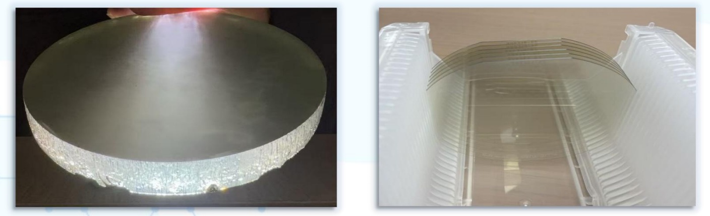
Until recently, high-quality AlN single-crystal substrates were dominated by a handful of overseas suppliers, creating a classic “money cannot buy” bottleneck for Chinese device makers. That picture has changed rapidly in 2026.
In Ningbo, Jingyaoshengsi and peer companies have moved from laboratory growth to stable 2-inch AlN production. One leading producer reports planned year-end capacity of 5,000 wafers per year, with a roadmap toward larger diameters and higher throughput. Key quality metrics now routinely achieved on product-grade (P-grade) material include:
• HR-XRD FWHM (002) ≤ 100 arcsec, (102) ≤ 80 arcsec
• Surface roughness (Al-face CMP) ≤ 0.5 nm
• Thickness uniformity and bow controlled to ≤ 30 µm on 2-inch wafers
• Available sizes: 10 × 10 mm, 1-inch, and 2-inch, offered in Product (P), Research (R) and Development (D) grades.
This is the same inflection point SiC experienced a decade ago: when domestic substrate supply becomes reliable, device design and epitaxy activity accelerate. The materials supply chain must keep pace.
3. The PVT Growth Challenge — Why Materials Matter at 2,000 °C+
Like SiC, commercial AlN bulk crystals are grown by Physical Vapor Transport (PVT). The process runs at extremely high temperature under carefully controlled nitrogen/argon atmospheres. Several hardware and consumable elements determine yield and quality:
Core growth container: crucible & source crucible
The reaction “heart.” High-purity graphite or refractory metals (W/Ta) are used, almost always with an internal tantalum carbide (TaC) coating to resist corrosive aluminum vapor. The source crucible holds the AlN powder charge and is engineered with multi-layer structures to control sublimation flux.
Seed mounting & orientation control
Precision seed holders keep the growth face exposed to the sublimation zone while maintaining exact crystallographic orientation. Even small angular errors propagate into mosaic structure and higher dislocation density.
Heating & thermal-gradient system
Medium-frequency induction coils or multi-zone resistance heaters establish the axial temperature gradient (typically 5–100 °C/cm) required for stable growth. Coil geometry, turn spacing and insulation screens (side, top and bottom) directly affect growth rate and crystal quality.
Gas handling & effusion systems
Precise N₂/Ar pressure control plus active effusion/exhaust paths remove excess species from the growth interface — a PVT-specific feature that improves surface morphology and reduces defects.
Every one of these elements consumes high-purity graphite, TaC- or CVD-SiC-coated components, and carefully sized high-purity AlN powder. As furnace utilization rises and diameters move from 2-inch toward 4-inch and beyond, both powder charge volume and component lifetime become critical cost and quality drivers.
4. High-Purity AlN Powder & Process Consumables — The Upstream Bottleneck
Crystal quality begins with the source material. Product-grade AlN powder for PVT must meet:
• Purity ≥ 99.95 %–99.999 % (5N class preferred)
• Ultra-low oxygen and metallic impurities
• Controlled particle-size distribution and high tap density (spherical or near-spherical preferred)
• Consistent batch-to-batch chemistry so that sublimation kinetics remain repeatable
On the hardware side, the same coated-graphite technology developed for SiC epitaxy and crystal growth transfers directly to AlN PVT furnaces: TaC-coated crucibles and susceptors, CVD-SiC coated graphite components, high-purity insulation, and long-life seed holders. Component lifetime under aluminum-rich vapor is still an industry challenge; incremental improvements in coating integrity and thermal-field design translate into higher furnace uptime and lower cost per wafer.
5. From AlN Substrates to the Broader Fourth-Generation Materials Ecosystem
AlN single-crystal substrates are only one part of the story. The same high-purity AlN powder also feeds:
• High-thermal-conductivity ceramic substrates and heat-spreaders
• Thermal interface fillers and structural ceramics
• Epitaxial templates and buffer layers for GaN and AlGaN devices
In parallel, high-transparency, high-thermal-conductivity SiC continues to serve dual optical + thermal roles in advanced packaging and high-power modules — a natural complement to AlN in the ultra-wide-bandgap toolkit.
6. Semixlab’s Role in the AlN & Ultra-Wide-Bandgap Supply Chain
Semixlab supplies the critical upstream materials and process consumables that keep high-temperature crystal growth and epitaxy running:
• High-purity SiC and related powder raw materials engineered for PVT and other sublimation processes, with purity and particle-size distributions matched to specific thermal profiles.
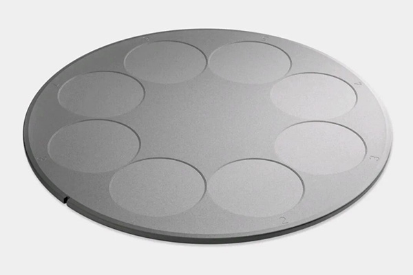
• CVD SiC- and TaC-coated graphite components — crucibles, susceptors, rings, wafer holders, pins and barrel susceptors — for crystal growth, epitaxy, RTP/RTA and ALD.
• Solid SiC components (showerheads, focus/edge/etch rings, wafer boats, cantilever paddles) for oxidation, diffusion and harsh plasma environments.
• Thermal-field insulation and high-purity graphite solutions that help maintain the tight temperature gradients demanded by both SiC and AlN PVT furnaces.
As the industry moves from 2-inch AlN demonstration to multi-inch volume production, the same materials discipline that enabled SiC’s scale-up will determine how quickly AlN reaches cost and quality parity. Semixlab works with substrate manufacturers, furnace builders and epitaxy houses to close that materials gap.
Looking Ahead
Fourth-generation semiconductors are no longer a laboratory curiosity. With domestic 2-inch AlN already in volume production and clear roadmaps to larger diameters, the materials supply chain is entering its next expansion phase. High-purity powders, long-life TaC- and SiC-coated graphite, and precision thermal-field hardware are the quiet enablers behind every additional wafer that leaves the growth furnace.
For device designers targeting the highest voltages, the deepest UV wavelengths, or the most extreme thermal environments, AlN is becoming a practical option. For materials suppliers, it is the next demand curve after SiC — and the companies that master the 2,000 °C+ consumables will capture durable value.
About Semixlab
Semixlab supplies advanced materials and process consumables for critical stages of wide- and ultra-wide-bandgap semiconductor manufacturing:
• High-purity raw materials for PVT crystal growth
• CVD SiC- and TaC-coated graphite susceptors, crucibles, rings and holders
• Solid SiC components for high-temperature and plasma processes
• Thermal insulation and graphite solutions for crystal-growth furnaces
Visit: www.semixlab.com
References & Further Reading
1. Product specifications: 10×10 mm, 1-inch and 2-inch AlN single-crystal substrates (P/R/D grades), high-purity AlN powder, high-transparency SiC — 2026 product literature.
2. Industry reports on domestic 2-inch AlN mass production and capacity plans (Ningbo-based producers, 2026).
3. Material property data compiled from published literature on AlN bandgap, breakdown field and thermal conductivity.
4. PVT growth hardware and thermal-gradient practices drawn from public technical discussions of AlN and SiC crystal growth.
© 2026 Semixlab · www.semixlab.com · CVD SiC / TaC coated graphite · High-purity raw materials · Solid SiC components
Table of Contents
- Why Aluminum Nitride Is the Fourth-Generation Semiconductor
- Domestic Breakthrough: 2-Inch AlN Single-Crystal Mass Production
- The PVT Growth Challenge — Why Materials Matter at 2,000 °C+
- High-Purity AlN Powder & Process Consumables — The Upstream Bottleneck
- From AlN Substrates to the Broader Fourth-Generation Materials Ecosystem
- Semixlab’s Role in the AlN & Ultra-Wide-Bandgap Supply Chain
- Looking Ahead
- About Semixlab
- References & Further Reading
Founded in 2018, Semixlab Technology Co.,Ltd is a technology-based enterprise focusing on the research and development, production and sales of advanced materials. It is a world-leading semiconductor material manufacturer.