EN
 EN
 DA
 NL
 FI
 FR
 DE
 IT
 JA
 KO
 NO
 PL
 PT
 RO
 RU
 ES
 SV
 TL
 ID
 SK
 UK
 VI
 TH
 TR
 FA
 BE
 LA
 UZ
In brief: Electric vehicles powered SiC's first major growth curve. Now NVIDIA's August 2026 AIDC 2.0 white paper is positioning 800VDC as the power standard for AI factories. For the SiC industry, this could be a second "Tesla moment"—and the demand curve may rise even faster.
1. NVIDIA AIDC 2.0 and the 800VDC AI Data Center Power Architecture
NVIDIA's AIDC 2.0 white paper, published in August 2026, sets out 800VDC high-voltage direct current as the power standard for next-generation AI factories. The proposed architecture combines 34.5kV medium-voltage direct feed, modular power blocks, and solid-state protection to move far more power through the data center efficiently.
The reason is simple: rack power is climbing almost vertically—from 330 kW for Rubin to 570–660 kW for Rubin Ultra/Kyber, and toward roughly 1 MW in native 800V architectures. That is 5–10 times the 10–20 kW racks common only five years ago. At 54V, the required current, copper volume, and I²R losses quickly become unmanageable. Moving to 800V cuts current to about one-sixteenth, shifting system value away from copper and magnetic components and toward SiC power semiconductors. In other words, silicon advances as copper retreats. The clearest example is the SiC-based solid-state transformer (SST), a market projected to grow from USD 169 million in 2024 to USD 936 million by 2030, representing a 32% CAGR.
2. Grid-to-Chip Power Conversion: How SiC and GaN Divide the AI Data Center Power Chain
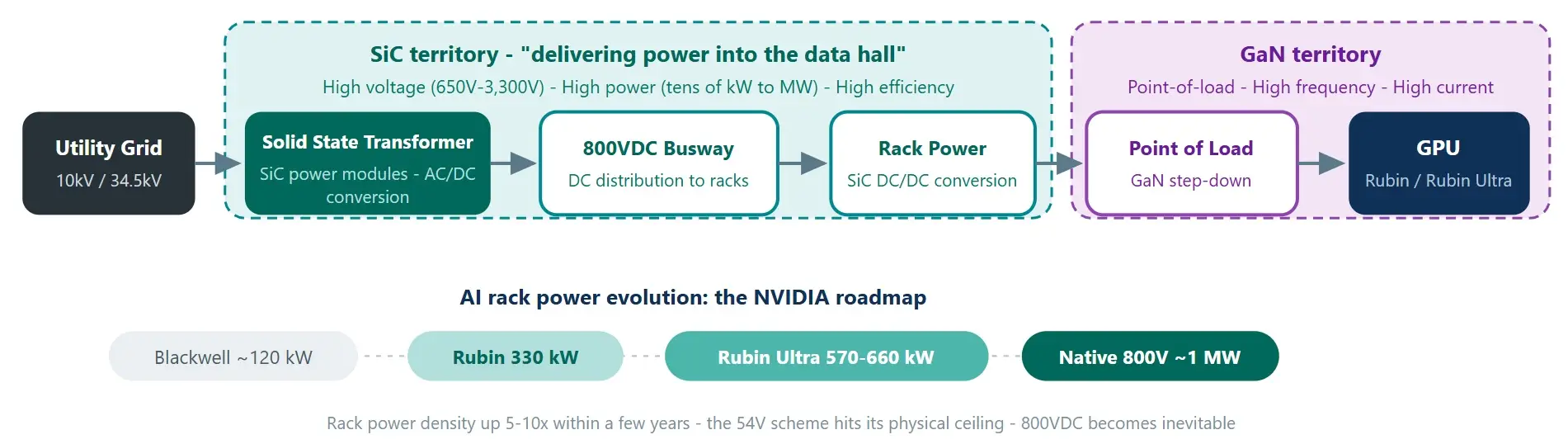
Figure 1: Grid-to-Chip power chain. SiC brings high-voltage power into the data hall; GaN performs the final high-frequency step-down near the GPU.
SiC controls the first half of the chain. Utility power at 10–34.5kV passes through SiC-based solid-state transformers and into 800VDC busways that feed the racks. This is a kilovolt-class, megawatt-scale segment where SiC's material properties matter: its 3.26 eV bandgap and critical electric field—about ten times that of silicon—enable efficient operation under high voltage and high power density.
GaN takes over in the second half, where high-frequency point-of-load converters step voltage down close to the GPU. Qingchun Semiconductor captures the division of labor well: SiC delivers power into the data hall; GaN feeds the chips. The company also reports that its SiC devices are already shipping in volume for AI data center applications.
SDIC Securities estimates that AI power supplies could account for 50% of the SiC power device market by 2030, translating into roughly RMB 34 billion in substrate demand. That would create an EV-scale market—but on a potentially steeper adoption curve.
Why Silicon Carbide Must Dominate High-Voltage AI Data Center Power?
The case is rooted in materials physics. Compared with conventional silicon devices, SiC offers order-of-magnitude advantages in three areas: higher breakdown field, lower switching losses, and reliable operation at higher temperatures. Together, these properties make smaller, more efficient power conversion possible at the voltage and power levels required by AI factories.
| Key parameter (4H-SiC vs Si) | SiC | Si | Engineering significance |
| Bandgap | ≈3.26 eV | ≈1.12 eV | High-temperature, radiation-tolerant operation; long-term reliability at higher junction temperatures |
| Critical breakdown field | ≈10× Si | Baseline | Thinner drift regions and lower on-resistance at equal voltage ratings—the fundamental source of high-voltage conversion efficiency |
| Thermal conductivity | ≈3× Si | Baseline | Superior heat extraction: lower cooling system cost and volume |
3. SiC Substrate Manufacturers Pivot to AI Data Center Demand
White papers show where the market is heading; earnings reveal whether the shift is real. SICC (Tianyue Advanced) reported record Q2 2026 revenue of RMB 548 million and returned to profitability. The company held a 51.3% share of China's 8-inch conductive substrate market and ranked first globally with a 27.6% share. Two developments stand out. First, its 12-inch substrates entered volume delivery, completing a 6-, 8-, and 12-inch portfolio, while AI data centers were named explicitly as a core application—an important first for a leading substrate manufacturer. Second, crystal growth furnaces for volume production are now sourced domestically, strengthening the local supply loop from raw material to boule.
The capacity race is accelerating. Jingsheng's 8-inch project targets 900,000 wafers per year, while Silan and Sanan continue to ramp their lines. China's SiC industry is moving beyond prototyping into volume delivery, but that transition depends on something less visible: a stable upstream supply of high-purity raw materials and long-life process consumables.
4. High-Purity SiC Raw Materials and Epitaxy Consumables: The 2,300°C Bottleneck

Figure 2: Each additional megawatt of rack power ultimately drives material charging and component replacement in SiC crystal growth furnaces and epitaxy reactors.
Every SiC power device begins with two demanding high-temperature processes.
PVT crystal growth (>2,300°C): High-purity SiC powder sublimates and recrystallizes on a seed at a growth rate of less than 1 mm per hour. The material requirement is recurring because fresh powder is charged for each run, so consumption rises directly with furnace utilization. A purity of 5N (≥99.999%) is the practical survival line: impurities can increase micropipes and dislocations, reducing boule quality and yield. As the industry moves from 6-inch to 8-inch and 12-inch substrates, charge volumes grow and particle-size control becomes tighter—an easily overlooked cost behind the capacity race.
SiC epitaxy (1,500–1,650°C): CVD SiC - or TaC-coated graphite susceptors support the wafers, couple RF heating, and help shape the reactor's temperature field. Temperature uniformity directly affects epitaxial layer quality, while coating integrity influences particle generation and maintenance intervals. The move to 8-inch and 12-inch wafers raises the bar again, requiring redesigned thermal fields, tighter flatness control, and longer component life.
The chain is direct: every additional megawatt envisioned in NVIDIA's white paper travels from the power system to SiC devices, then to substrates, and finally to high-purity SiC raw materials and epitaxy consumables. Data center power growth therefore becomes tangible demand for crystal growth furnaces, powder charges, coated graphite components, and reactor replacement parts.
5. From NVIDIA 800VDC AI Data Centers to SiC Material Demand
In just eight years, SiC's growth story has expanded from vehicle electrification to AI compute. The second curve could be both steeper and longer: demand is no longer tied only to EV traction inverters, but increasingly to the power infrastructure behind AI. As that demand moves upstream—from devices to substrates, raw materials, and consumables—the most resilient opportunities may sit at the critical material nodes that keep the entire chain running.
About Semixlab
Semixlab supplies SiC materials and process consumables for critical stages of semiconductor manufacturing:
· High-purity SiC raw material for PVT crystal growth, with purity and particle-size distributions tailored to specific processes;
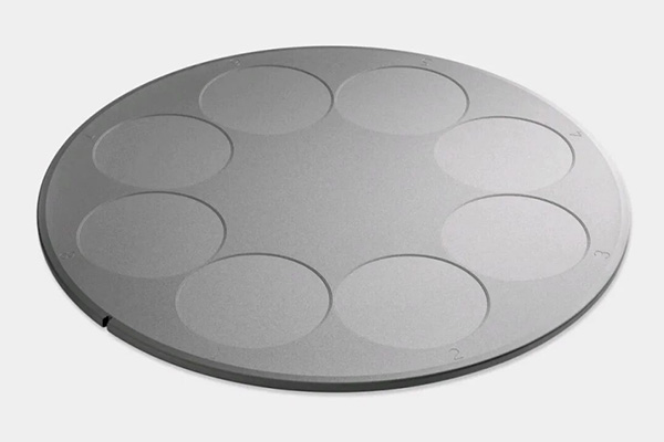
· CVD SiC- and TaC-coated graphite susceptors, epitaxy rings, wafer holders, pins, and barrel susceptors for epitaxy, RTP/RTA, and ALD processes;
· Solid SiC components—including showerheads and focus, edge, and etching rings—plus SiC wafer boats and cantilever paddles for oxidation and diffusion.
As SiC's growth story expands from EVs to AI compute, we work with substrate manufacturers, epitaxy houses, and equipment suppliers to bring greater materials-side certainty to the power backbone of the AI era.
Visit: www.semixlab.com
Table of Contents
- NVIDIA AIDC 2.0 and the 800VDC AI Data Center Power Architecture
- Grid-to-Chip Power Conversion: How SiC and GaN Divide the AI Data Center Power Chain
- SiC Substrate Manufacturers Pivot to AI Data Center Demand
- High-Purity SiC Raw Materials and Epitaxy Consumables: The 2,300°C Bottleneck
- From NVIDIA 800VDC AI Data Centers to SiC Material Demand
- About Semixlab
Founded in 2018, Semixlab Technology Co.,Ltd is a technology-based enterprise focusing on the research and development, production and sales of advanced materials. It is a world-leading semiconductor material manufacturer.