EN
 EN
 DA
 NL
 FI
 FR
 DE
 IT
 JA
 KO
 NO
 PL
 PT
 RO
 RU
 ES
 SV
 TL
 ID
 SK
 UK
 VI
 TH
 TR
 FA
 BE
 LA
 UZ
Overview
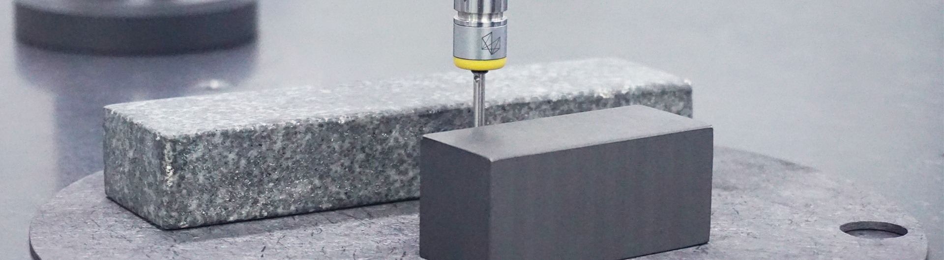
| Industry | Semiconductor Wafer Fabrication, Photovoltaic Single Crystal Pulling Equipment, Microelectronics Epitaxial Growth & Diffusion Reaction Chambers |
| Process | Physical Acid Washing & Distillation of High-Purity Natural Ore, Trichlorosilane (TCS) Vapor Phase Distillation & Deposition, High-Temperature High-Pressure Hydrothermal Quartz Crystal Growth |
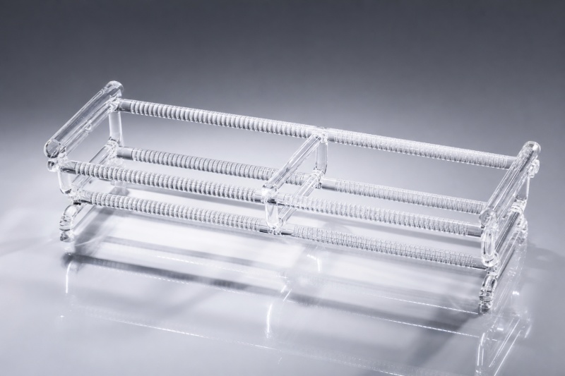
| Solution | 6N Grade (99.9999%) Ultra-High Purity Quartz Structural Components, Hydrothermal Synthetic Quartz Ingots, High-Purity Quartz Diffusion Tubes & Boat Holders |
| Services | Precision Machining of Quartz Parts per Engineering Drawings, Factory ICP-MS Metal Impurity Spectroscopy Test Reports (TDS), Clean Vacuum Packaging |
| Results | Achieved total metal impurities below 0.1 ppm (strictly controlled alkali and transition metals), excellent high-temperature creep resistance, providing customers with a stable domestic substitution option. |
Key Abstract & Introduction
Semiconductor wafer diffusion and epitaxial processes require quartz components (wafer boats, diffusion tubes, reaction chambers) to achieve 6N grade (99.9999%) purity, strictly controlling the impact of alkali and transition metal diffusion on the electrical performance of wafers. In the face of supply volatility from natural high-purity ore sources (such as Spruce Pine), overcoming impurity and high-temperature creep challenges through vapor phase distillation purification and hydrothermal crystal synthesis provides equipment OEMs and wafer fabs with a highly reliable, fully traceable high-purity quartz substitution solution.
1. Core Purity Requirements and Limitations of Natural Ore Sources
● Core Takeaway: Semiconductor wafer manufacturing imposes extremely high purity demands on quartz (6N grade). Traditional high-purity ore sources suffer from high geographic concentration and natural impurity limits, necessitating engineered solutions to overcome purification bottlenecks.
High-temperature diffusion, oxidation, and epitaxial growth processes in semiconductor manufacturing require quartz components to operate continuously at 1100°C–1200°C. If the quartz substrate contains excessive impurity elements, it will not only significantly lower the thermal softening point of the quartz (causing deformation under gravity at high temperatures) but also directly contaminate silicon wafers through thermal evaporation or vapor-phase migration. Specifically, semiconductor-grade high-purity quartz has extremely strict control metrics for various impurities:
· Alkali Metals (Na, K, Li): Typically require individual concentration control below 0.1–0.5 ppm. Alkali metal ions migrate very easily at high temperatures, posing a fatal threat to the electrical stability of the gate oxide layer in silicon wafers.
· Transition Metals (Fe, Cu, Ni, Cr): Concentrations must be restricted to within 0.1 ppm. Transition metals form deep-level impurity centers that drastically reduce carrier lifetime in silicon wafers.
· Bubbles & Microscopic Inclusions: In addition to chemical purity, internal micro-bubbles and grain boundary defects tend to cause stress concentration and even cracking during high-temperature annealing, affecting thermal field uniformity.
Historically, natural mineral deposits that meet the requirements for direct high-temperature melting into high-purity quartz have been extremely rare, relying primarily on the Spruce Pine mining district in North Carolina, USA. This dependence on a single geographical source makes the global semiconductor supply chain fragile when facing natural disasters or logistics bottlenecks, driving deep industrial R&D into chemical purification and synthetic quartz processes.
2. Mainstream Purification & Synthesis Technologies for Semiconductor High-Purity Quartz
● Core Takeaway: Chemical vapor phase transformation purification (TCS distillation) and hydrothermal high-pressure crystal growth are currently the two mainstream technological routes to achieve 6N-grade high-purity quartz.
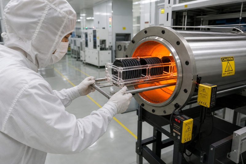
To break free from the bottleneck of uneven impurity content in natural vein quartz ores, modern semiconductor quartz engineering mainly adopts two core process routes:
1. Vapor Phase Transformation Purification (TCS Distillation & Deposition Route)
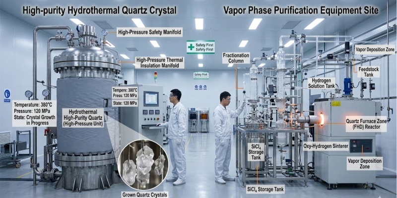
Vapor phase purification converts silicon-containing raw materials into volatile chlorosilane compounds (such as Trichlorosilane SiHCl₃ or Silicon Tetrachloride SiCl₄), using multi-stage distillation columns to eliminate trace metal chloride impurities based on boiling point differences. The purified high-purity gaseous silicon compounds undergo hydrolysis/pyrolysis in a high-temperature oxyhydrogen flame or plasma, generating high-purity silicon dioxide particles (Soot), which are then dehydroxylated at high temperature and densified into solid ingots. Due to the high separation selectivity of distillation columns, this method can stably reduce total metal impurities to the ppb level, producing synthetic fused quartz of ultra-high purity.
2. High-Temperature & High-Pressure Hydrothermal Crystal Growth
Hydrothermal growth simulates natural quartz crystallization in a specialized autoclave. Using lower-cost ordinary natural quartz as the nutrient raw material, it dissolves in alkaline hot water under high temperature (300°C–400°C) and high pressure (100–150 MPa), and slowly crystallizes onto oriented seed crystals in the growth zone to produce giant high-purity single crystals. The hydrothermal process leverages the difference in crystallization rates between impurities and the SiO₂ lattice to naturally reject impurities. The resulting synthetic quartz crystal exhibits low internal defects, making it suitable for high-precision photolithography lenses and ultra-demanding semiconductor diffusion holders.
Table 1: Technological Route vs. Performance Metrics Comparison
| Process Route / Technical Indicator | Traditional High-Purity Natural Ore Physical Acid Washing | Vapor Phase Distillation / Hydrothermal Synthetic Quartz |
| SiO₂ Purity Grade | 99.99% – 99.999% (4N–5N) | Above 99.9999% (6N Grade) |
| Total Metal Impurities (ppm) | < 20 – 50 ppm | < 0.1 – 0.5 ppm (ppb-level control) |
| Hydroxyl (OH-) Content Control | Dependent on natural minerals & melting process | Precisely adjustable via vacuum/chlorination annealing |
| Primary Semiconductor Scenarios | Conventional thermal diffusion tubes, outer chambers, wafer boats | Ultra-advanced process epitaxial chambers, lithography optics, ultra-clean internal parts |
3. Quartz Purification Cost & Domestic Supply Chain Substitution Solutions
● Core Takeaway: Although synthetic and advanced purification methods increase energy consumption and front-end costs, they significantly lower overall operating risks for wafer fabs by extending equipment lifespan and ensuring stable localized supply.
While vapor phase purification and hydrothermal synthesis reliably achieve 6N-grade purity, these processes come with relatively high energy consumption and long production cycles. For semiconductor equipment OEMs and wafer fabricators, striking a rational balance between performance requirements and cost efficiency is key to process selection:
• Energy Consumption & Waste Acid Treatment Costs:
Physical purification of natural ore requires large quantities of hydrofluoric acid (HF) and nitric acid across multiple deep acid-washing stages, involving complex environmental waste liquid treatment costs. In contrast, vapor phase distillation requires reaction deposition at high temperatures exceeding 1000°C, leading to higher energy expenditure. Factories effectively reduce unit purification costs through process waste acid recycling systems and cascading waste heat utilization.
• Diversified Breakthroughs in Domestic High-Purity Quartz Supply Chain:
In recent years, significant progress has been made in domestic high-purity quartz purification technology, with several local enterprises achieving commercial mass production in vapor-phase synthetic quartz and fine washing of high-purity ore. By establishing comprehensive ICP-MS (Inductively Coupled Plasma Mass Spectrometry) testing systems, manufacturers ensure that each batch of outgoing quartz structural components complies with customer engineering drawings, effectively mitigating the supply risk of over-reliance on a single overseas ore source.
4. Frequently Asked Questions & Customization Guide for High-Purity Quartz Components
● Core Takeaway: Providing objective and rigorous technical answers addressing customer key concerns regarding purity testing standards, high-temperature anti-creep selection, and batch delivery traceability.
Q1: What are the practical differences between 6N-grade synthetic quartz and 5N-grade natural high-purity quartz in diffusion furnace tube applications?
Answer: 5N-grade natural high-purity quartz exhibits stable performance and higher cost-effectiveness in most mature diffusion and oxidation processes above 28nm. However, in 14nm and more advanced nodes or highly sensitive epitaxial equipment, 6N-grade synthetic quartz eliminates wafer yield fluctuations caused by trace alkali metal drift and offers superior stability against thermal shock and cracking during long-term high-temperature operation.
Q2: How do you guarantee that delivered quartz components are free from trace metal contamination?
Answer: All finished semiconductor-grade quartz parts undergo high-purity acid pickling surface passivation, followed by ultrasonic cleaning and double-layer vacuum cleanroom packaging inside an ISO 5 (Class 100) cleanroom. Every product batch is shipped with an accompanying ICP-MS trace metal analysis report, ensuring full elemental impurity traceability.
Q3: Can cold machining and thermal fabrication of complex quartz chambers or wafer boats be customized according to our engineering drawings?
Answer: Yes. We are equipped with multi-axis CNC machines dedicated to quartz engraving and milling, oxyhydrogen flame fusion welding equipment, and precision annealing furnaces. We can process complex quartz structural parts based on customer engineering drawings and perform strict stress-relief annealing to prevent cracking in high-temperature environments.
Conclusion: Objective Evaluation of Material Characteristics to Build High-Reliability Quartz Value
Manufacturing semiconductor-grade quartz boats and wafer holders depends not only on the purification level of raw materials but also on downstream precision cold machining, flame fusion welding, and rigorous stress annealing control. We are committed to providing high-precision, low-deformation custom quartz boat solutions tailored to the specific thermal field conditions and wafer loading requirements of wafer fabs and equipment manufacturers.
Welcome to visit our Semiconductor-Grade High-Purity Quartz Wafer Boats & Holders Product Page to explore detailed specifications and carrier solutions, or check our High-Purity Quartz Components & Diffusion Tubes Category Page. If you need to evaluate component purity metrics, thermal field compatibility, or request a Technical Data Sheet (TDS), please feel free to contact our engineering technical team.
Table of Contents
- Overview
- Key Abstract & Introduction
- Core Purity Requirements and Limitations of Natural Ore Sources
- Mainstream Purification & Synthesis Technologies for Semiconductor High-Purity Quartz
- Quartz Purification Cost & Domestic Supply Chain Substitution Solutions
- Frequently Asked Questions & Customization Guide for High-Purity Quartz Components
- Conclusion: Objective Evaluation of Material Characteristics to Build High-Reliability Quartz Value
Founded in 2018, Semixlab Technology Co.,Ltd is a technology-based enterprise focusing on the research and development, production and sales of advanced materials. It is a world-leading semiconductor material manufacturer.