EN
 EN
 DA
 NL
 FI
 FR
 DE
 IT
 JA
 KO
 NO
 PL
 PT
 RO
 RU
 ES
 SV
 TL
 ID
 SK
 UK
 VI
 TH
 TR
 FA
 BE
 LA
 UZ
1. The Evolutionary Timeline
• 1970s–1980s: Pioneering Semiconductor Epitaxy: Researchers at Union Carbide Corporation introduced high- purity SiC-coated graphite susceptors into the epitaxial growth of Gallium Nitride (GaN) and Silicon (Si). This innovation solved the acute outgassing and thermal degradation problems of uncoated graphite in reactive
semiconductor chambers, enabling high-performance optoelectronic LEDs and RF power devices.
• 2000s–Present: Modern High-Precision Thin Films: Advancements in physical vapor deposition (PVD), plasma- enhanced chemical vapor deposition (PECVD), and reactive sputtering have facilitated nanoscale silicon carbide coatings. Modern semiconductor fabrication relies heavily on high-purity CVD SiC coatings for MOCVD, SiC epi- reactors, etching chamber focus rings, and high-temperature thermal processing carriers.
2. Crystallographic Polymorphism: Superiority of Cubic β-SiC Coatings
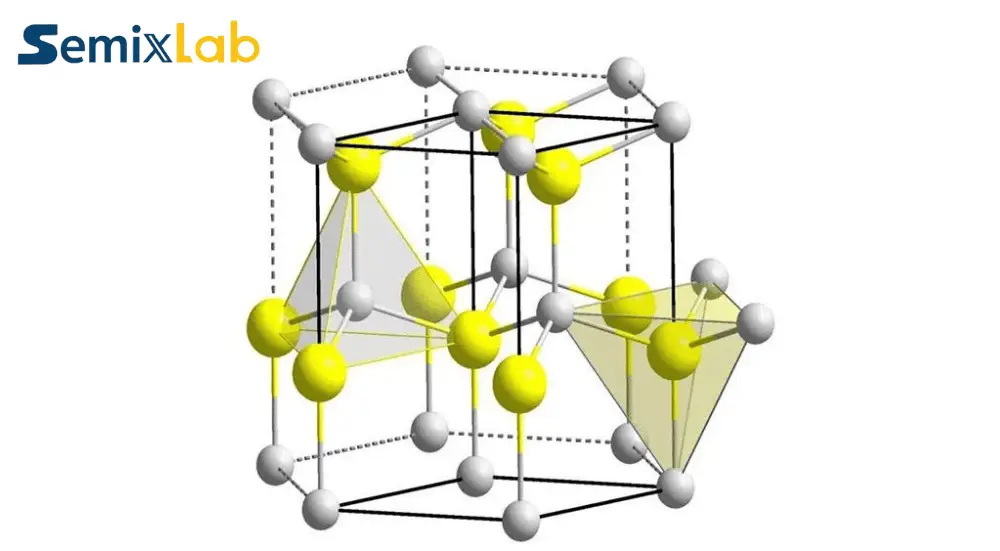
Silicon Carbide exhibits pronounced polymorphism, with over 200 distinct polytypes. These polytypes are broadly divided into two major thermodynamic phases based on atomic stacking sequences:
• α-SiC (Alpha Phase): The high-temperature stable polytype (e.g., 4H-SiC, 6H-SiC, 15R-SiC) featuring hexagonal or rhombohedral crystal symmetry. While single-crystal 4H-SiC substrates dominate power electronics (MOSFETs,
Schottky diodes) due to wide bandgap properties, bulk α-SiC suffers from crystalline defects when applied as heterogeneous thin films.
• β-SiC (Beta Phase / 3C-SiC): The low-temperature stable cubic structure synthesized around 1450°C. Above 2100°C–2400°C, β-SiC transforms into α-SiC. β-SiC coatings are universally preferred for protective surface coatings on specialty graphite components due to critical physical advantages:
KEY PHYSICAL ADVANTAGES OF Β-SIC COATINGS:
• Superior Thermal Conductivity: β-SiC achieves isotropic thermal conductivities of 120–200 W/(m·K), exceeding standard α-SiC polycrystalline forms (100–140 W/(m·K)), enabling rapid thermal response and uniform heat distribution.
• Enhanced Mechanical Micro-Hardness: Cubic β-SiC provides exceptional resistance against particle erosion, mechanical abrasion, and plasma ion bombardment inside etch and CVD chambers.
• Broad Chemical & Thermal Stability: While α-SiC degrades in aggressive alkaline environments at elevated temperatures, β-SiC exhibits complete chemical inertness across strong oxidizing acids, chlorine, ammonia, and strongly alkaline atmospheres.
• CTE Matching with Graphite: The Coefficient of Thermal Expansion (CTE) of cubic β-SiC (α ≈ 4.5 × 10⁻⁶ / K) tightly matches that of high-density, isotropic, fine-grain specialty graphite, preventing coating delamination, micro-cracking, and thermal fatigue during rapid thermal cycles.
3. Technological Comparison of SiC Coating Deposition Methods
Selecting the optimal deposition route determines coating stoichiometry, density, adhesion strength, and thermal shock tolerance. Below is a comparative engineering evaluation of major industrial processes for synthesizing Silicon Carbide Coatings:
| Deposition Method | Key Mechanics & Precursors | Main Advantages |
| Chemical Vapor Deposition (CVD) | High-temperature reaction of gas precursors at 1100–1400°C. | Ultra-high purity (>99.999%), 100% theoretical density, strong chemical bonding. |
| Physical Vapor Deposition (PVD) | Magnetron sputtering or electron-beam evaporation under ultra-high vacuum conditions. | Low process temperature, precise nanoscale thickness control, excellent optical-grade density. |
| Thermal Spraying Techniques | Plasma or high-velocity oxy- fuel (HVOF) spraying of melted/semi-melted SiC micro-powders. | High deposition rate, cost-effective for large-area structural components. |
| Electrochemical Deposition | Electro-crystallization of silicon/carbon precursors from molten salt or organic liquid solutions. | Non-line-of-sight coating on complex conductive substrates, low temperature requirement. |
| Slurry Coating & Sintering | Dip/spray liquid slurry containing SiC powders and organic binders, followed by high-temperature sintering. | Simple equipment requirement, low operational cost, suitable for thick protective coatings. |
4. Critical Applications: SiC-Coated Graphite Susceptors in MOCVD & Semiconductor Epitaxy
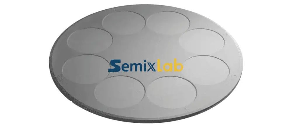
In high-end epitaxy growth—such as Gallium Nitride (GaN-on-SiC, GaN-on-Si) and Silicon carbide epitaxial growth for power electronics—the substrate holder, known as a graphite susceptor, is exposed to extreme temperatures (1000°C– 1600°C), aggressive corrosive gases (NH3, H2, HCl, Silane), and rapid thermal ramps. Unprotected graphite outgasses carbon impurities and undergoes chemical etching, destroying semiconductor yield.
Applying an ultra-high purity CVD SiC coating to specialty graphite susceptors addresses these processing bottlenecks through five critical engineering functions:
1. High-Purity Structural Barrier & Carbon Sealing
Isostatic graphite naturally contains micro-pores and residual metallic contaminants (ash content ~10–20 ppm). A dense, non-porous CVD SiC protective layer completely seals the porous graphite base, blocking the outgassing of carbon dust, trace sulfur, and metal impurities into the epitaxy chamber. This ensures ultra-clean wafer growth environment necessary for high electron mobility transistors (HEMTs) and micro-LEDs.
2. Chemical Resistance against Hydrogen and Ammonia Etching
During GaN MOCVD epitaxy, high concentrations of hot ammonia (NH3) and carrier hydrogen (H2) severely etch exposed carbon substrates, causing surface pitting and structural distortion. The cubic β-SiC coating exhibits complete chemical inertness to atomic hydrogen and nitrogen cracking species up to 1600°C, extending susceptor lifetime significantly.
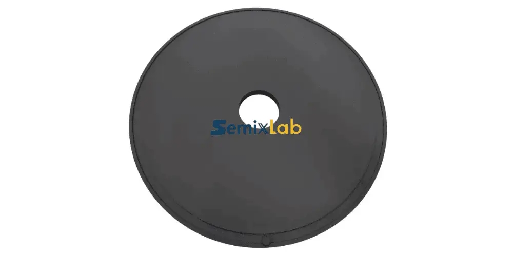
3. Optimized Thermal Uniformity & Temperature Gradient Control
Wafer lattice perfection requires precise temperature uniformity across 6-inch, 8-inch, or larger wafer carriers (ΔT < 1°C). The high thermal conductivity of the isotropic CVD SiC coating layer eliminates local hot spots, facilitating rapid, homogeneous radiative and conductive heat transfer across pancake, barrel, and 3D rotational wafer susceptors.
4. Lattice and Interface Strain Management
Tailoring the deposition parameters of β-SiC thin films (stoichiometry, crystallographic grain orientation, and internal stress) allows engineers to tune the thermal expansion match between the susceptor and the wafer/carrier interface. This reduces mechanical warping during cooling and improves film yield.
5. Superior Wear and Corrosion Resistance during Cleaning Cycles
MOCVD and epitaxy chambers undergo frequent in-situ gas cleanings using aggressive halogen gases (NF3, Cl2, HCl). High-density silicon carbide coatings resist chemical degradation and physical sputtering, preventing premature degradation of precision wafer pockets.
5. Future Trends & Industry Outlook
As the semiconductor industry advances toward 200mm (8-inch) SiC epitaxial growth and ultra-wide bandgap devices (Gallium Oxide β-Ga2O3, Aluminum Nitride AlN), coating demands are intensifying:
• Intelligent & Automated CVD Processing: Real-time optical emission spectroscopy (OES) and automated gas-ratio tuning are being integrated into CVD reactors to achieve sub-micron film thickness uniformity across complex 3D susceptors.
• Ultra-High Purity & Zero-Defect Control: Modern SiC coating standards demand metallic impurity levels below 0.1 ppm and defect-free crystal domain growth to eliminate particle generation.
• Hybrid Ceramic Coatings (SiC / TaC Dual-Layers): For high-temperature SiC epitaxy (>1500°C), hybrid structures combining CVD SiC with Tantalum Carbide (TaC) outer layers are emerging to withstand hydrogen etching while maintaining high thermal responsiveness.
Founded in 2018, Semixlab Technology Co.,Ltd is a technology-based enterprise focusing on the research and development, production and sales of advanced materials. It is a world-leading semiconductor material manufacturer.